Replicant: Reproducing a Fault Injection Attack on the Trezor One
Overview
There has been a lot of public work in the last four or five years surrounding the security of cryptocurrency wallets. Much of this research has been in the realm of fault injection, which is the art/science of disrupting an embedded system just enough that it will cause undefined behavior to occur. The goal is to find a fault that allows one to modify the device's behavior to grant an attacker escalated levels of access. Examples of this might include skipping instructions, corrupting memory read operations, etc.
Goals
This post aims to provide a road map and example of how to replicate a fault injection attack and the hurdles and shortcomings that can occur when attempting to do so. Furthermore, by outlining the process of replicating one of these attacks, we hope that readers come away from this post more confident in generating their own fault injection attacks or replicating pre-existing work.
But before we dive into all that, let's briefly review what fault injection (FI) is and outline some resources you can use to get started in this space.
A Brief Primer on Fault Injection
Fault injection involves introducing an error/modification minor enough to cause undefined behavior on a target but not enough to stop the target from operating entirely. This typically involves injecting a high voltage pulse or temporarily draining the voltage from a targeted power source or "rail" on the target system.
By causing momentary voltage modulations (either above or below the expected voltage), we can force our target system to enter a realm of undefined behavior. An adequately targeted fault can bypass various security checks or other features that may impede an attacker or reverse engineer.
With regards to the common fault injection methods, there are a few different types of faults that we can try to introduce: clock glitching and voltage glitching.
Clock Glitching
With clock glitching, our goal is to skip or modify instructions. The idea is that by injecting another clock cycle, we can cause the processor to skip over an instruction.
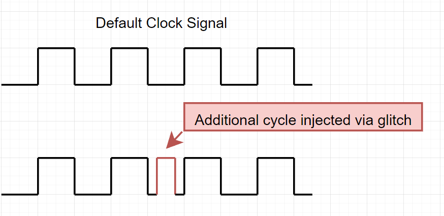
As you can probably imagine, these need to be precise as we try to modify or manipulate a specific sequence of clock cycles to get our desired outcome. Clock glitching targets the external clock on a CPU or microcontroller with the end goal of injecting a clock signal at the appropriate time, causing an instruction to be skipped.
Voltage Glitching
Voltage glitching involves targeting the power source of the entire system. By briefly cutting the power to a target system, we can modify its behavior/performance.
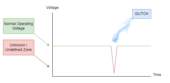
With voltage glitching, our goal is to reduce the voltage for a short enough time such that the processor does not entirely shut down but instead enters an undefined state or causes some type of undefined behavior. Unfortunately, this task does not come easy as many processors are specifically designed to avoid this scenario, sometimes requiring an attacker to get creative with component removal or injection methods.
If you want to learn more about these methods, I cannot recommend the NewAE materials highly enough. Even if you don't have a chipwhisperer at home, their tutorials, forums and documentation are perfect for anyone wanting to learn more about fault injection.
Electromagnetic Fault Injection
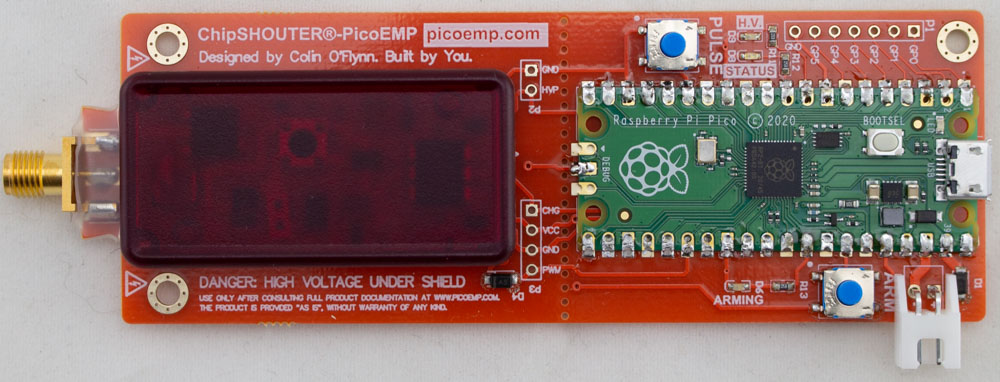
We can also inject faults into our targets using something like the PicoEMP or chipshouter, these tools inject faults in a different way than the two methods mentioned above.
These tools are used to perform EMFI (electro-magnetic-fault-injection) attacks. These attacks involve generating a large electric field that can cause hardware to fail, resulting in potential bit-flips and other undefined behavior. For more information on EMFI attacks, check out Colin O'Flynn's excellent talk on the same wallet we will review with this post.
Now that we are a little more familiar with the ideas behind fault injection let's talk about the attack replicated in this post. This post aims to replicate the work presented in the chip.fail presentation. This work outlines the process of using fault injection to bypass an RDP check in the bootrom of the STM32F2 series MCU, allowing the attacker to access the device's internal memory via SWD. This is the same attack that was recently replicated by Joe Grand to recover a large amount of currency from the wallet. Before we get into the details of the attack, let's start by examining our target device and learning more about its security features.
Target Overview
The target for this work is the Trezor One wallet. This is a popular low-cost wallet that is built around the STM32F2 microcontroller. Trezor's hardware and software are both open source, this is great because it gives us access to the hardware diagrams and the firmware source, which will help eliminate a lot of reverse engineering work.
The Trezor One utilizes the STM32F2 MCU; before we move on, let's review some of the relevant CPU features.
STM32 Security Overview
Multiple security features can be enabled on an STM32 microprocessor; a brief description can be found below.
-
RDP 0 - Flash unlocked, all-flash/ram is accessible via the debug interface
-
RDP 1 - Flash locked; you can connect a debugger and read out RAM/peripherals, but not flash.
-
RDP 2 - Flash locked, RAM reads locked, debug interface locked
Our target has protection level RDP2 enabled, so we need to find a way around that; to do that, we have to take a slightly closer look at how power is managed and regulated within the STM32.
STM32 Power Management/Regulation
Within any microcontroller, there are multiple power domains; these are used for powering various chip peripherals and internal operations and comparators. We will be targeting the internal voltage regulator. A brief overview of the power domains in the STM32 can be seen below:

This diagram shows that the VCAP_1 and VCAP_2 lines give us a direct path to the internal regulator, affecting things like kernel logic, flash memory, and IO logic. So if we can briefly manipulate this line, we can hopefully affect how these peripherals behave!
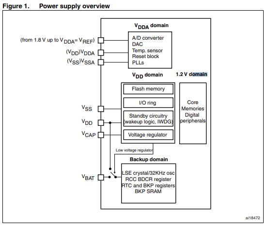
For this work, we will be targetting the internal voltage regulator by attempting to manipulate the VCAP lines shown in the image above. Why are we targeting this line? Or more importantly, how can we find similar voltage rails to target other processors when we move on to additional targets for fault injection?
The VCAP lines ensure that all internal comparators and regulators are appropriately managed. If we can manipulate this line, we can potentially alter the behavior of the CPU's core memories and digital peripherals and cause undefined/modified behavior. Hopefully, glitching this internal regulator (perhaps during a specific memory operation involving the RDP settings) will allow us to modify the device's RDP state.
To recap, we want to attempt to modify the RDP state of the device from RDP2 to RDP1, and we want to do so by glitching or briefly interrupting the voltage supplied on the
VCAP_1/VCAP_2 lines are used to help regulate the internal voltage regulator. If we can modify the behavior of the internal voltage regulator, we can potentially alter the processor's behavior. Now that we have reviewed our target's internal security features and the power rail we will target, let's talk about the specifics of the attack.
The Attack
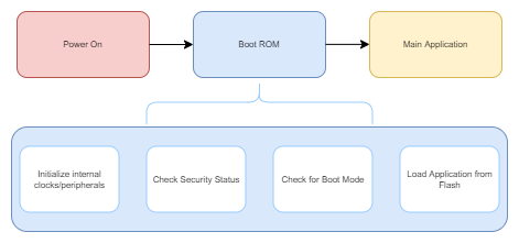
This work aims to replicate the research presented in the chip.fail research, which resulted in the discovery of a bug in the bootrom of the STM32F2 microcontroller. For those that may not be familiar, the bootrom is responsible for handling a lot of the early startup functionality of the microcontroller (similar to a BIOS on your modern computer). The bootrom is responsible for performing basic peripheral initialization, security checks, boot mode checks, and finally loading the main application into memory and executing it. A high-level outline of the boot process can be seen below:
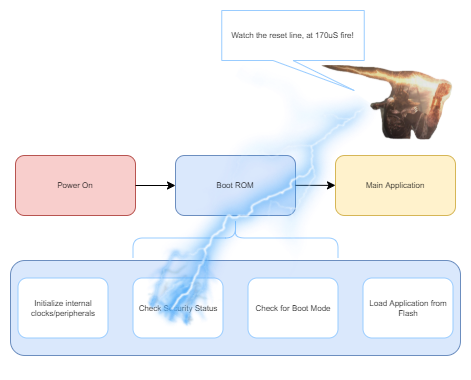
With the chip.fail research; It was discovered that if an attacker could inject a fault roughly 170 microseconds after the processor began executing its bootrom, an RDP check could be bypassed. This would allow an attacker to drop the STM32 from RDP2 to RDP1, allowing SRAM access via SWD. Additionally, the recovery keys could be extracted by reading SRAM, allowing access to the wallet's contents. (Note: Trezor has mitigated this bug by removing the recovery keys from RAM in updated firmware versions).
The attack:
- Power on the wallet
- When the RESET line is asserted, begin the countdown to the glitch
- At 170 microseconds, pull VCAP low
- Test RDP bypass via SWD
- Read SRAM from the target device
If step 4 is successful and the wallet continues booting, the glitch is successful, and the internal SRAM can be read out of the target.
So what does an attack like this look like at the signal level? How do we know when the processor has started executing the boot ROM? How would one proceed if analyzing a new target/power trace? Let's start by removing a few components from our target and looking at a power trace.
Preparing our Target
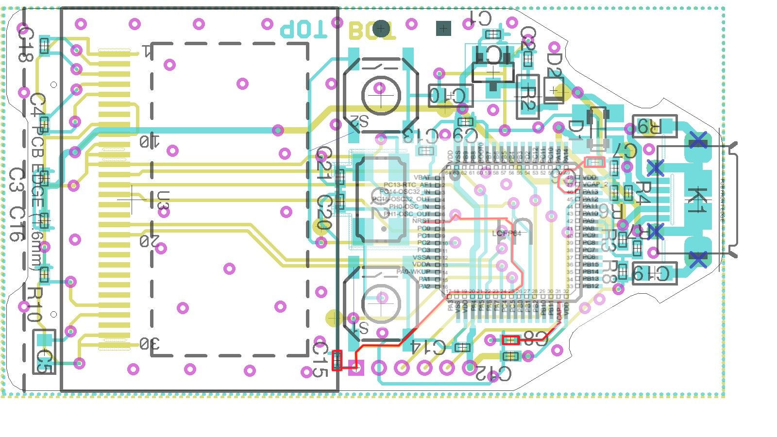
To make sure that our glitch is as effective as possible, we need to remove the external capacitors connected to the VCAP lines and the reset line. This can be done with a standard soldering iron and some patience. These capacitors (highlighted in the schematic below) are used to ensure that the voltage remains stable, which is what we don't want when doing fault injection.
Below is the default schematic for the Trezor One:
The highlighted components in red below outline capacitors that need to be removed.
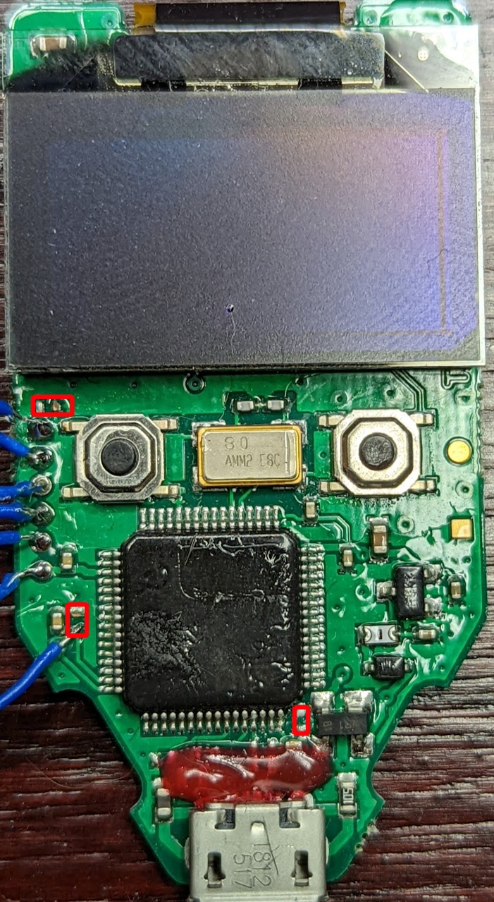
Below is an image of the wallet with the removed capacitors highlighted in red:
Capturing Power Traces
Now that we have identified the components that need to be removed and the lines we care about, we need to capture some example power trace data. To do this, we will use an oscilloscope. For our research, we used the Siglent SDS1104X-E 100Mhz Digital Oscilloscope and a standard DC measurement probe included with the scope.
When performing power captures like this, it is essential to make sure that you have your oscilloscope set up correctly. We configured our scope to trigger on the reset line using a rising edge trigger. This means the scope will begin capturing when it detects the reset line rising.
It is essential to take some time when dialing in your triggers for your oscilloscope. While it may be tempting to use something like continuous capture, or "Rolling" mode, this will drastically decrease your capture rate and result in less granular power traces. For the samples we will be reviewing later, our sample rate was 500MSa/s.
It should also be noted that we were not using a shunt resistor when we captured our traces; an article about how to properly utilize shunt resistors for power measurement can be found here.
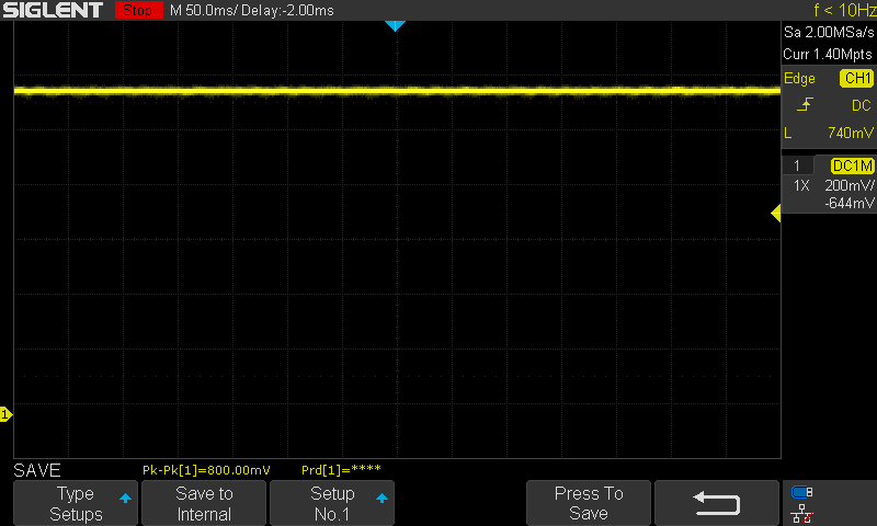
Next, let's review some example power traces. Below is an example view of the voltage on the VCAP line with the external capacitors:
Here is the same line with the capacitors removed:
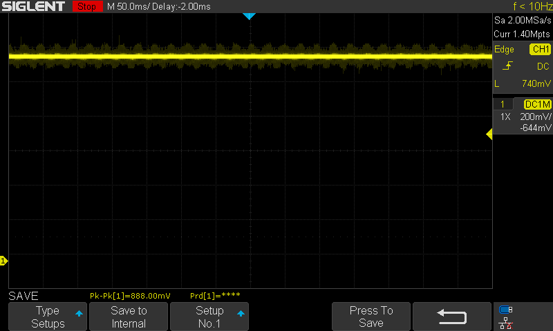
Notice that the line is now much noisier and less stable; this is what we want when attempting to inject a fault or a glitch onto a power rail. With our capacitors removed and our test pads soldered, let's perform some initial power analysis, starting with our target line (VCAP) as it relates to the RESET line. The bootrom begins execution when the system reset line hits the 3.3V threshold. Thus by monitoring the reset line, we can determine when the boot ROM begins execution; we will use this as our trigger for our glitch.
The pink line represents the voltage on the VCAP line, while the yellow line is the voltage on the RESET line:
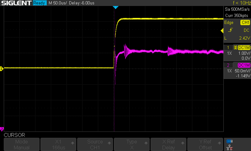
We can see various activity regions highlighted in the gif below; notice the voltage fluctuations in these regions. Based on how this MCU boots, we can make some assumptions about what these multiple fluctuations mean.
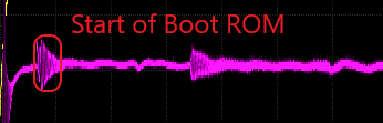
While our trace may look different than the one highlighted in the original research, we can see that our capture is similar in terms of the structure of the power trace. For example, if we look at our trace at roughly 170 microseconds, we can see the flash activity before the main application begins execution.
Now that we have removed the relevant capacitors, we next need to connect to the SWD port. This can be accessed through the vias on the right of the PCB, as shown in the image below:
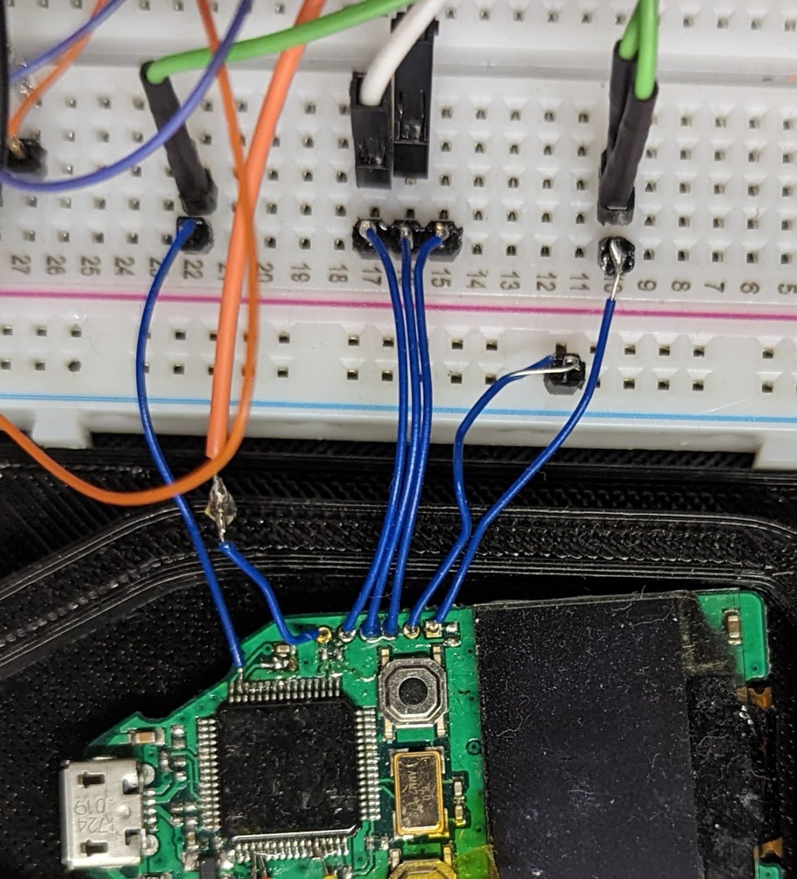
With these lines broken out to a breadboard, it's time to replicate the attack.
Replicating the Attack
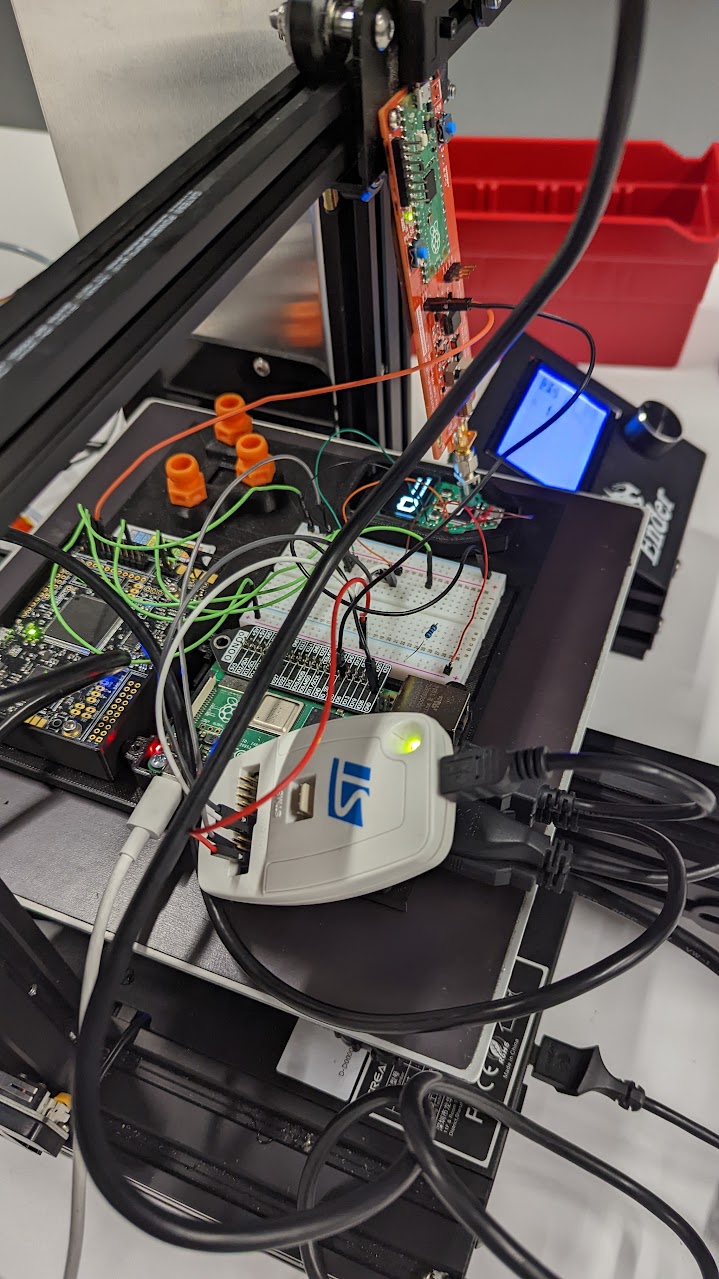
For this work, we 3d printed a jig for the components, shown in the image below:
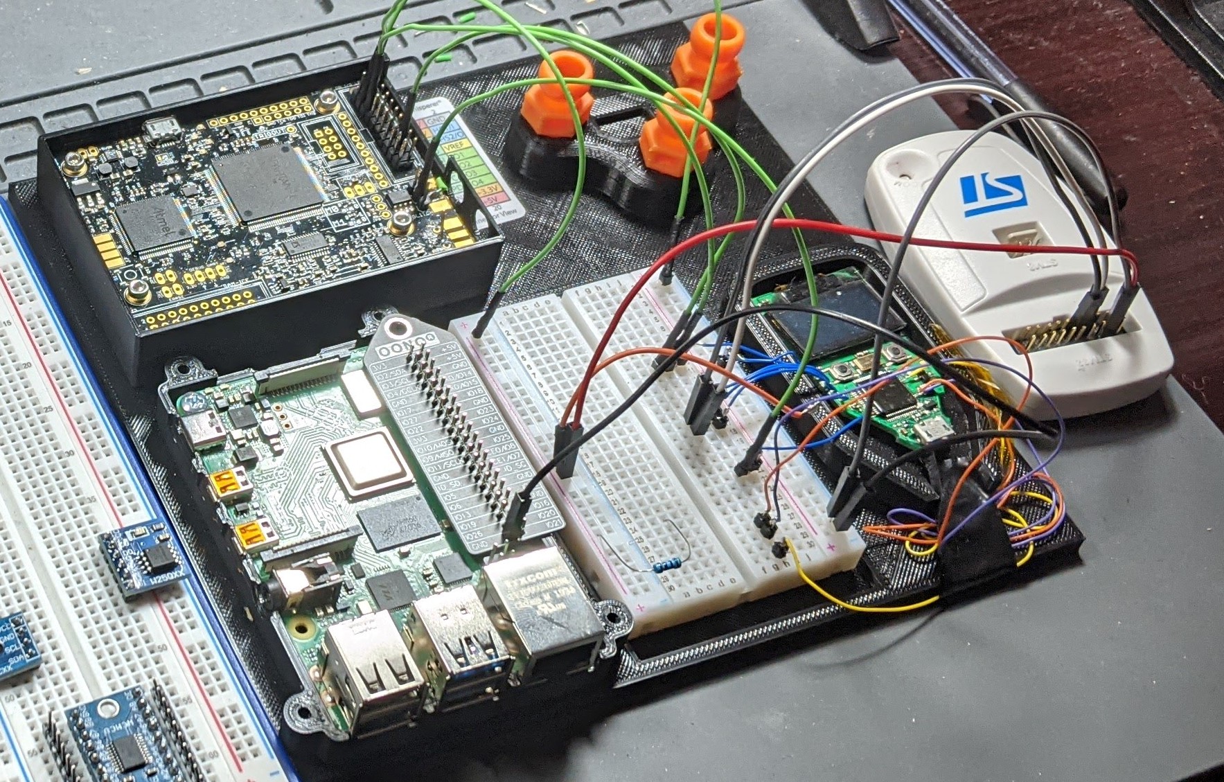
The STL file can be found in the GitHub repo here
Hardware
For our setup, we used a Raspberry Pi, ChipWhisperer and STLink. The STLink was connected to the SWD port of the Trezor and is what we use to detect that the RDP bypass has been performed successfully. The ChipWhisperer is used to power the wallet, trigger the reset line, and glitch the VCAP line. A simple wiring table for our setup can be seen below:
| ChipWhisperer Pin Number / Usage | Trezor Pin |
|---|---|
(14) / FPGA-TARG4 |
RST |
(5) / PROG-RESET |
RST |
Glitch Out |
VCAP1 |
(3) / +3.3V |
VCC |
(2) / GND |
GND |
| STLink Header | Trezor Pin |
|---|---|
GND |
VDD |
SWCLK |
PA14 |
SWDIO |
PA13 |
VTREF |
VCC |
Software
With all the appropriate connections made, it is time to interface with the ChipWhisperer and dial in the parameters of our desired glitch. As mentioned before, the NewAE tutorials are a great place to start, and we used this notebook as a template for our attack.
A few key things need to be dialed in when working with the chip whisperer, and we'll walk through some of them now. The referenced code can be found here.
The overall flow of the program is simple:
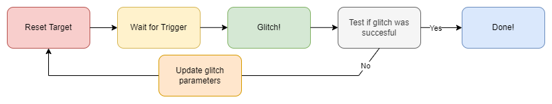
Let's start with connecting to our CW; this can be done with the following code:
import chipwhisperer as cw
scope = cw.scope()
We need to make sure that we set the internal clock frequency of the CW as well as the output mode and trigger source; we do this with the following lines:
scope.glitch.clk_src = "clkgen" # set glitch input clock
scope.glitch.output = "enable_only" # glitch_out = clk ^ glitch
scope.glitch.trigger_src = "ext_single" # glitch only after scope.arm() called
Next, let's talk about triggering. We mentioned before that we would use the reset line to indicate when the boot ROM begins executing. This line will also be used to reset the target if the glitch is unsuccessful and needs to be rerun.
# Trigger on IO4. This is connected to our reset line
scope.trigger.triggers = 'tio4'
The reboot_flush function is responsible for completely resetting the device and arming the glitch. We will call this function whenever we want to reset the STM32 and test new glitch parameters:
def reboot_flush():
    global scope
    # Cut power to target device
    scope.io.target_pwr = False
    # Pull reset low
    scope.io.nrst = False
    # Set up CW for glitching
    scope.arm()
    # Put reset in high impedance mode (we are triggering off of it)
    scope.io.nrst = "high_z"
    # Power the target and wait for the glitch to trigger
    scope.io.target_pwr = True
Next, we will define our glitch parameters; we will do this using the GlitchController class as shown below:
gc = glitch.GlitchController(groups=["success", "failure"], parameters=["width", "offset", "ext_offset"])
gc.set_global_step(g_step)
gc.set_range("width", 40, 40)
gc.set_range("offset", -45, -45)
gc.set_range("ext_offset", 15000, 18000)
scope.glitch.repeat=20
These last three lines are essential for our glitch's time and the shape.
Shaping the Glitch
The three variables we use to help shape our glitch are the width,repeat, and offset variables. Note that these definitions are pulled from the Newaetech Tutorials. It should also be noted that many things can affect the shape of our glitch in addition to these variables such as wire length and quality. As a general rule of thumb using short shielded wires with SMA connectors is best practice.
width: How wide to make the glitch. This is the percentage of one period. For our example, we will use the maximum value as we are doing voltage glitching, not clock glitching.repeat: The number of clock cycles to repeat the glitch. Higher values increase the number of instructions that can be glitched but often increase the risk of crashing the target. Note: a higher repeat typically results in a stronger glitchoffset: Where in the output clock to place the glitch.
These three variables can be manipulated to shape our glitch; we can change the width and overall strength of the glitch. Next, we have to determine when we trigger the glitch relative to some external signal on our target, which in our case will be the RESET line.
Timing the Glitch
The final range definition ext_offset defines how many clock cycles the FPGA will wait after triggering before performing the glitch. Since we previously specified a clock rate of 100 MHz, 15000 clock cycles equate to approximately 150 microseconds. This means that after the RESET line goes high on the Trezor, we will start counting down from our ext_offset value, and when it hits zero - we will glitch the VCAP line!
Another thing to note is that the GlitchController class will iterate over all of the glitch parameters provided. So for each possible combination of parameters we will be resetting the wallet, attempting the gitch and then attempting to connect to the STM32 via SWD. This means that for testing large ranges of values we may need multiple days to finish a series of tests.
We ran the first iteration of the glitch while monitoring with the scope and saw that our glitch was generated correctly. We let the glitch run over the weekend and were looking forward to returning to the office victorious with an active SWD port on our Trezor.
Debugging the Attack
After running the attack for some time with no results, we began troubleshooting our setup. The first thing we wanted to debug was our STLink SWD enumeration code that was being used to detect a successful glitch:
'''
swd_check
Use the link to attempt to connect via SWD
'''
def swd_check():
    global dev
    import swd
    pc = 0
    try:
        dev = swd.Swd()
        pc = dev.get_version().str
    except:
        del swd
        pass
    return pc
First, we tested the detection of a successful glitch by using an STM32 dev board at RDP level 0, which immediately worked on the first iteration.
This was a good sign, but we wanted to test what would happen when we called the swd_check function multiple times.
Upon doing so, we found out that after the swd library fails to enumerate a device (which would happen on a failed glitch attempt), it would not work again until the STLink had been re-enumerated via USB!
This meant that for all of our tests, only our first iteration was properly testing for SWD using the STLink. If it failed once, SWD would not work again until the probe had been unplugged and plugged back over USB!
Armed with this new knowledge and confident that we found our issue, we modified a simple c program to reset the STLink device after each glitch attempt.
'''
swd_check
Use the link to attempt to connect via SWD
'''
def swd_check():
    global dev
    import swd
    pc = 0
    try:
        # Reset the STLink
        os.system(f"sudo /home/pi/glitch/replicant/python/usbreset {usb_path}")
        dev = swd.Swd()
        pc = dev.get_version().str
    except:
        del swd
        pass
    return pc
With this, we were certain that we'd found our issue. Everything else looked great and lined up with the public literature; what else could go wrong? But unfortunately, we were still not seeing results after a few more days of testing and tweaking glitch parameters.
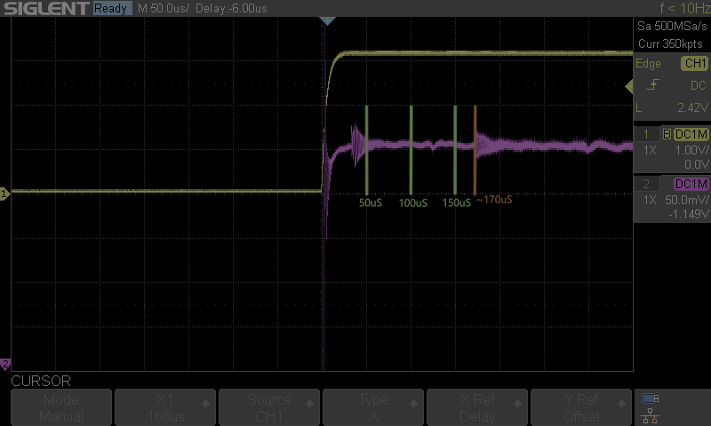
Finally, we decided to get the scope back out and inspect our glitch. We examined the glitch with an ext_offset of 16000,17000, and 18000, and it looked reasonable to the naked eye. However, with an ext_offset of 0, we saw the following:
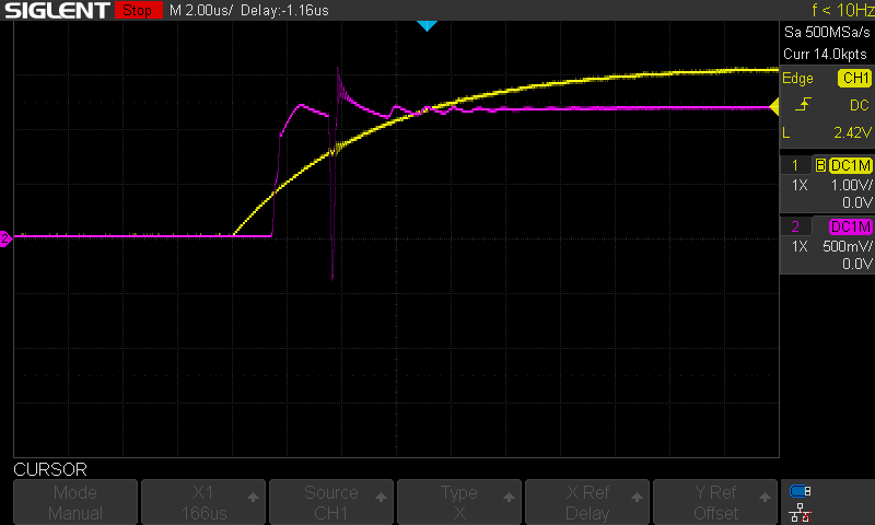
In the screenshot above, the yellow line is our RST line, and purple is the VCAP line. Note the gap between the glitch and the reset line reaching its target voltage. The ChipWhisperer is triggering before the reset line reaches 3.3V. This early triggering was causing our glitch to start counting down before the reset line was fully asserted. This was causing the glitch to trigger about 20 microseconds too early.
We can calculate the exact delay using the cursors on the oscilloscope, as seen in the image below:
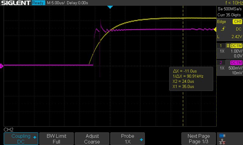
We determined we were triggering approximately 24 microseconds too early using the oscilloscope. Armed with this new information, we modified our ext_offset range to be between 17000 and 20000 and left that running over the weekend.
When we returned to the office on Monday, the STLink LED was green, meaning it had successfully accessed the device via SWD!
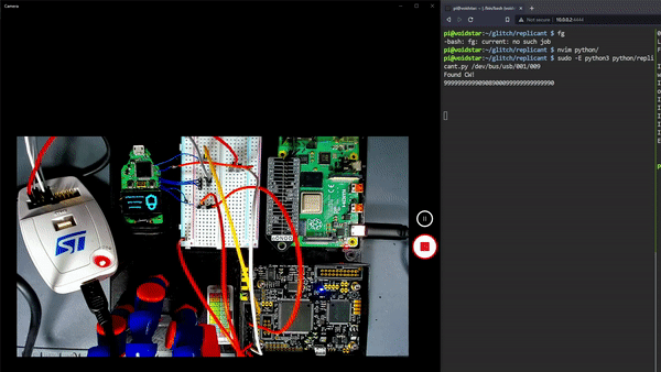
pi@voidstar:~/glitch/replicant $ sudo -E python3 python/replicant.py /dev/bus/usb/001/004
Found CW!
Success! -- offset = -44.921875, width = 39.84375, ext_offset = 19752
successes = 1, failures = 0, offset = -44.921875, width = 39.84375, ext_offset = 19752
Done glitching
Even more interesting is that our glitch hit around 197 microseconds after the ChipWhisperer triggered. Recall that in the chip.fail work; their offset was roughly 170 microseconds. Ours had a delay of 24 microseconds, placing it in a similar range to the previous research (197-24 = 173). This offset range was repeatable, and we could consistently trigger the glitch in the 194-197 microseconds range.
We can now use OpenOCD to read the SRAM region with the glitch.
pi@voidstar:~/glitch/replicant $ ./run_openocd.sh
Open On-Chip Debugger 0.10.0+dev-01514-ga8edbd020-dirty (2022-03-01-19:24)
Licensed under GNU GPL v2
For bug reports, read
        http://openocd.org/doc/doxygen/bugs.html
Info: auto-selecting first available session transport "hla_swd". To override use 'transport select <transport>'.
Info : The selected transport took over low-level target control. The results might differ compared to plain JTAG/SWD.
Info : Listening on port 6666 for tcl connections
Info : Listening on port 11111 for telnet connections
Info : clock speed 1000 kHz
Info : STLINK V2J29S7 (API v2) VID:PID 0483:3748
Info : Target voltage: 3.259749
Info : stm32f2x.cpu: hardware has 6 breakpoints, 4 watchpoints
Info : starting gdb server for stm32f2x.cpu on 3333
Info : Listening on port 3333 for gdb connections
Info : accepting 'telnet' connection on tcp/11111
With OpenOCD running, we can connect to it via telnet and read out SRAM:
pi@voidstar:~/glitch/replicant $ telnet localhost 11111
Trying ::1...
Trying 127.0.0.1...
Connected to localhost.
Escape character is '^]'.
Open On-Chip Debugger
> dump_image sram2.bin 0x20000000 0x1FFFFFFF

> exit
Connection closed by foreign host.
pi@voidstar:~/glitch/replicant $ hexdump -n512 -C sram2.bin
00000000  00 00 00 00 00 00 00 00  00 00 00 00 00 00 00 00  |................|
*
00000090  78 77 00 08 90 77 00 08  ff ff 00 00 13 70 00 08  |xw...w.......p..|
000000a0  1f 70 00 08 26 70 00 08  24 00 00 00 28 00 00 00  |.p..&p..$...(...|
000000b0  00 01 04 00 01 00 00 00  00 00 00 00 00 01 57 49  |..............WI|
000000c0  4e 55 53 42 00 00 00 00  00 00 00 00 00 00 00 00  |NUSB............|
000000d0  00 00 00 00 80 c3 c9 01  00 87 93 03 00 00 00 00  |................|
000000e0  00 00 00 00 00 00 00 00  00 00 00 00 00 00 00 00  |................|
*
00000200
A struct is present in the RAM dump that can be found at the following lines of code:
if (req->wIndex ==
USB_WINUSB_REQ_GET_COMPATIBLE_ID_FEATURE_DESCRIPTOR) {
    static const uint8_t winusb_wcid[] = {
        // header
        0x28, 0x00, 0x00, 0x00, // dwLength
        0x00, 0x01, // bcdVersion
        0x04, 0x00, // wIndex
        0x01, // bNumSections
        0x00, 0x00, 0x00, 0x00, 0x00, 0x00, 0x00, // reserved
        // functions
        0x00, // bInterfaceNumber - HACK: we present only interface 0 as
        // WinUSB
        0x01, // reserved
        'W', 'I', 'N', 'U', 'S', 'B', 0x00, 0x00, // compatibleId
        0x00, 0x00, 0x00, 0x00, 0x00, 0x00, 0x00,
        0x00, // subCompatibleId
        0x00, 0x00, 0x00, 0x00, 0x00, 0x00, // reserved
    };

    wait_random();
    USBD_CtlSendData(dev, UNCONST(winusb_wcid),
    MIN_8bits(req->wLength, sizeof(winusb_wcid)));
    return USBD_OK;

} else {
    wait_random();
    USBD_CtlError(dev, req);
    return USBD_FAIL;
}
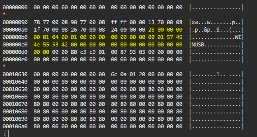
The image above shows the structure highlighted in an SRAM dump. We have successfully replicated the glitch and re-enabled the SWD peripheral.
Conclusion
This work and post aimed to demonstrate the difficulties and technical hurdles that can occur when attempting to replicate a fault injection attack. We demonstrated the process of using fault injection to bypass an RDP check in the bootrom allowing for an attacker to gain privileged access. This post demonstrates that small details matter when replicating a FI attack, and these details can change based on your hardware setup. All of the code and resources that were generated for this work can be found here
You might be asking yourself, is there a way we could do this without connecting to the VCAP lines and removing those additional capacitors? Keep an eye out for part two of this post, where we build on the knowledge gained from this post and demonstrate this same attack but with a PicoEMP:
If you are interested in this type of hardware-level reverse engineering, check out our training course or reach out to us for any consulting needs. If you want to get notified when a new blog post, course, or tool is released, consider signing up for the mailing list. I only send emails when there are actual posts or course updates. Lastly, you can follow me on twitter for various updates on side projects and classes.
This work was done alongside my friends Cody Gallagher and Aaron Phelps (LI/twitter), between the three of us we had a lot of fun replicating this attack. We also have to give a massive shout out to @stacksmashing and @colinoflynn who were very helpful and answered many of our early questions.
If you're interested in hardware security training at your organization, please don't hesitate to contact us. We also have a self-paced training available here
If you want to stay informed about official releases, new courses, and blog posts, sign up for our mailing list here.
References / Resources
Talks / Resources / References
- Thomas Roth (stacksmashing) FI Talk
- wallet.fail
- chip.fail
- Colin's Blog
- Chipwhisperer Tutorials
- Kraken Blog
- Joe Grand's Wallet Hacking
- STM32F2 Power Information
- STM32F2 Datasheet
Tools Used
To replicate this attack, one will need the following:
- Chipwhisperer Lite
- Python environment capable of installing the chipwhisperer package
pip install chipwhisperer
- Trezor One
- STLink Programmer
- Oscilloscope
- We used a Siglent Technologies SDS1104X-E
- Soldering equipment for component removal, etc