Overview
If you have ever needed to dissect network communications before, there is a good chance you have come across Scapy. Scapy is a Python networking library that allows for dissecting and crafting packets, sniffing Ethernet traffic, and even has a wide variety of support for various automotive protocols.
(Author's Note: Definitely check out their automotive documentation if you want to learn more about diagnostic protocols; it is an excellent resource.)
What a lot of us (myself included) don't remember when working with Scapy is that it is also a general-purpose binary protocol framework. Its detailed system for structuring, crafting, and dissecting packets does not care whether the bytes came via Ethernet, CAN or some other network protocol. In this blog post, we'll demonstrate how to use Scapy to dissect SPI traffic from a logic analyzer and reconstruct a firmware image from nothing but those captures.
Background Information
A few weeks ago, we were tasked with looking at an embedded device that we were only able to acquire one of. If you have been working in this space for a while, you know that this can be a challenge. With only one device, we don't want to risk damaging it by removing ICs, or even worse, triggering some sort of tamper protection. While tamper protection was not an identified concern on the device, we still thought that this would be a good excuse to develop some new tooling. Due to the nature of the exercise, we are not able to share a teardown of the device, but we can share the type of SPI flash that this device was using:
| # | Part | Type / Role | Datasheet |
|---|---|---|---|
| 1 | Winbond W25Q128JV |
SPI NOR flash, 16 MiB | Datasheet |
As is tradition when doing any embedded assessment, our first attempts at identifying UART and debug interfaces came up empty. The developers did a reasonable job of disabling diagnostic output and removing debug interfaces, and our attempts to read the flash in-circuit ran into some of the classic issues that we've covered before.
This was a black-box analysis, and we were not provided firmware for this target, which is pretty standard for a lot of our clients. While we've written a number of one-off scripts for reconstructing firmware from SPI captures, we wanted to take some time and develop some reusable tooling that we can share and improve upon in the future.
Before we go any further, let's do a quick refresher on how SPI works as a protocol, and how that protocol is leveraged to talk to SPI flash devices.
SPI: A Quick Refresher
SPI is a four-wire, full-duplex bus that shows up all over embedded systems. For a flash chip, the four core signals we care about are:
| Signal | Role |
|---|---|
CLK |
Clock, driven by the host (controller) |
CS / CS# |
Chip select, active low - frames a single transaction |
MOSI (DI) |
Controller → flash (commands, addresses, write data) |
MISO (DO) |
Flash → controller (read data, status) |
An important thing to remember as we go through this blog post is that chip select frames a transaction. Every time CS# goes low, a new command begins; when it goes high again, that command is done. Within that window the host clocks out an opcode, optionally an address, optionally some dummy cycles, and then either sends or receives data. Because SPI is full-duplex, MOSI and MISO are clocked at the same time - so during a read, the host is shifting out don't-care bytes on MOSI while the flash shifts out real data on MISO.
If you want the ground-up version of how SPI works on real hardware, we covered that in a previous post. It is also important to remember that SPI isn't only for flash; the same bus carries TPM traffic, sensor data, display commands, and plenty of proprietary protocols. By using Scapy to analyze this traffic, it is easy to add application-layer parsing in Python.
In the next section, we'll review some of the data that we captured on boot, and some of the interesting setbacks that we saw with this specific device.
SPI Traffic in Practice
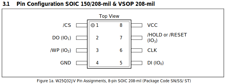
The part that we are interested in for this exercise uses a SOIC8 footprint which can be seen in the image below (the figure is from the W25Q32JV datasheet, but the SOIC8 pinout is shared across the W25Q family, including our W25Q128JV):
Using a SOIC8 clip and the Saleae Logic software, we can capture the signals sent to and from this chip on startup. Let's take a look at an initial capture together. This was collected by placing the clip and powering on the device:
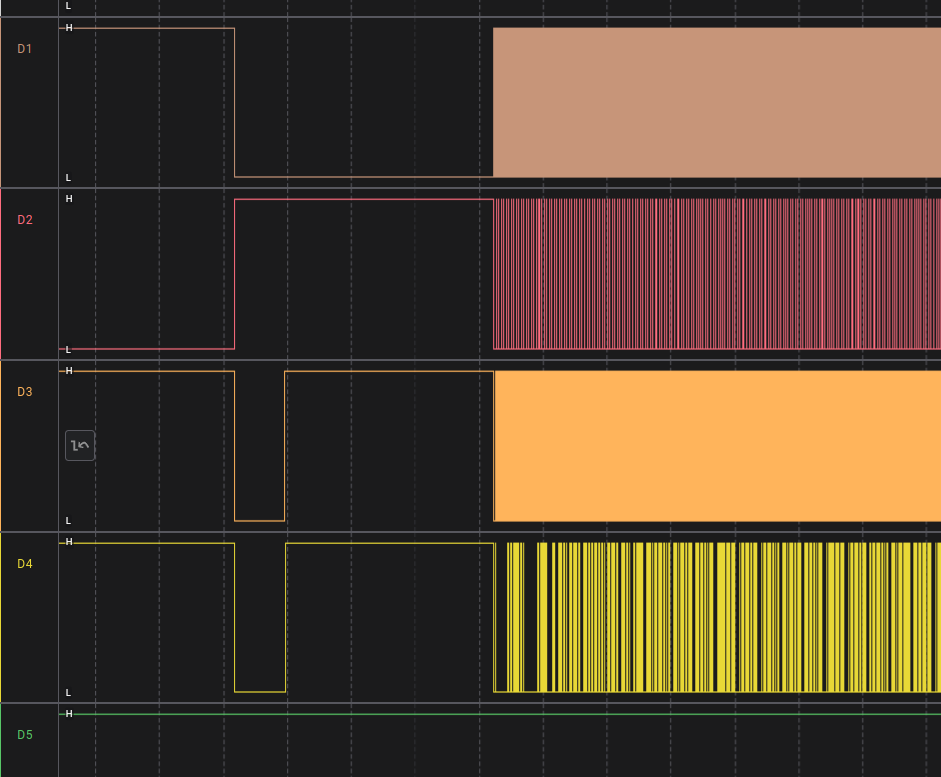
Note: This will not always work; oftentimes adding a clip and additional jumper wires will cause signal integrity issues at high speeds. Keep this in mind if you attempt this technique.
So we have some traffic, which is great. In this scenario, we know the exact pinout of the device, so we can map the Dx channels to their relevant signals, but what if we didn't have a pinout and we were just looking at a random debug header?
If we zoom in a little closer on the signals, we can see the following:
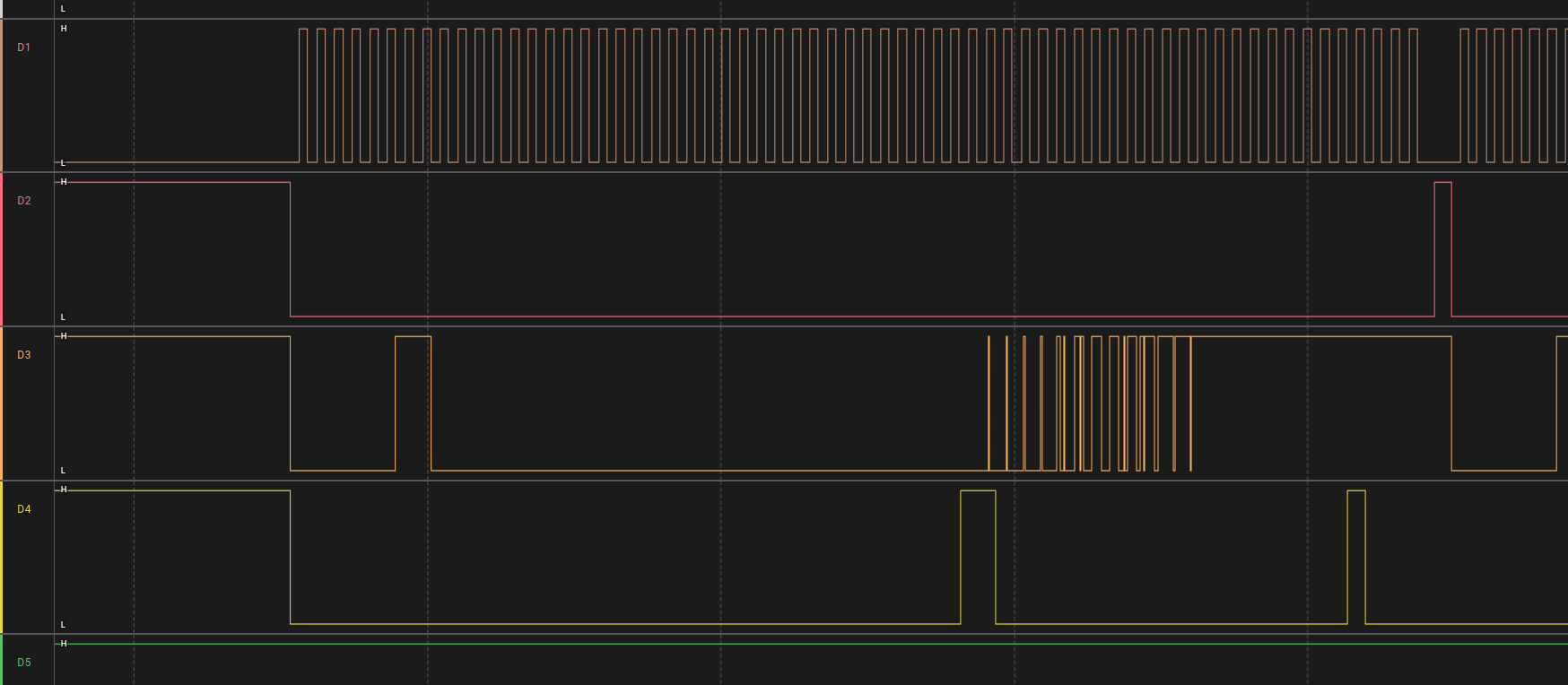
We know that SPI has four main signals, CS, CLK, DI and DO. Looking at this capture, we can see that the line connected to D1 is periodic, and measuring it gives us a frequency of 16 MHz. It is safe to assume that it's our clock line!
Moving down the line, notice that all activity starts when D2 goes low. If you recall from our refresher earlier, the CS line is used to determine the beginning of a SPI transaction. D2 goes low, then we see a clock signal generated. Note that D3 and D4 also go low around the same time, and shortly after that we start to see activity on both of them. Most importantly, all traffic stops when D2 goes high:
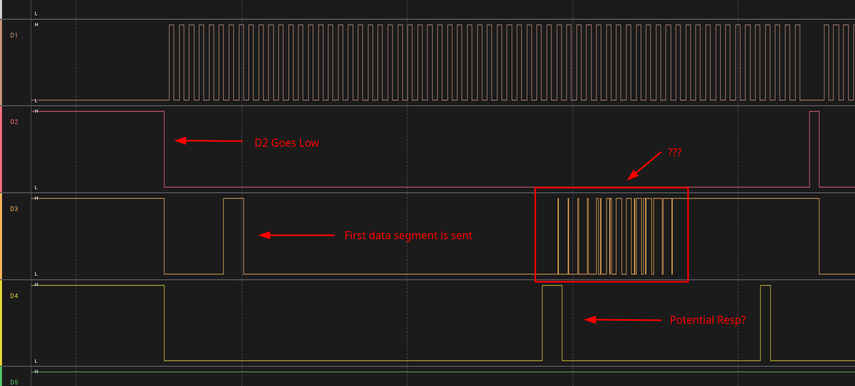
In the annotated image above, we can see that D3 is the first to transmit anything over the wire. Then shortly after that we see some data sent on D4. Note that we also have what appears to be some sort of noise on D3 when D4 becomes active. How do we know this is noise? Let's zoom in on the noisy region and take a look:
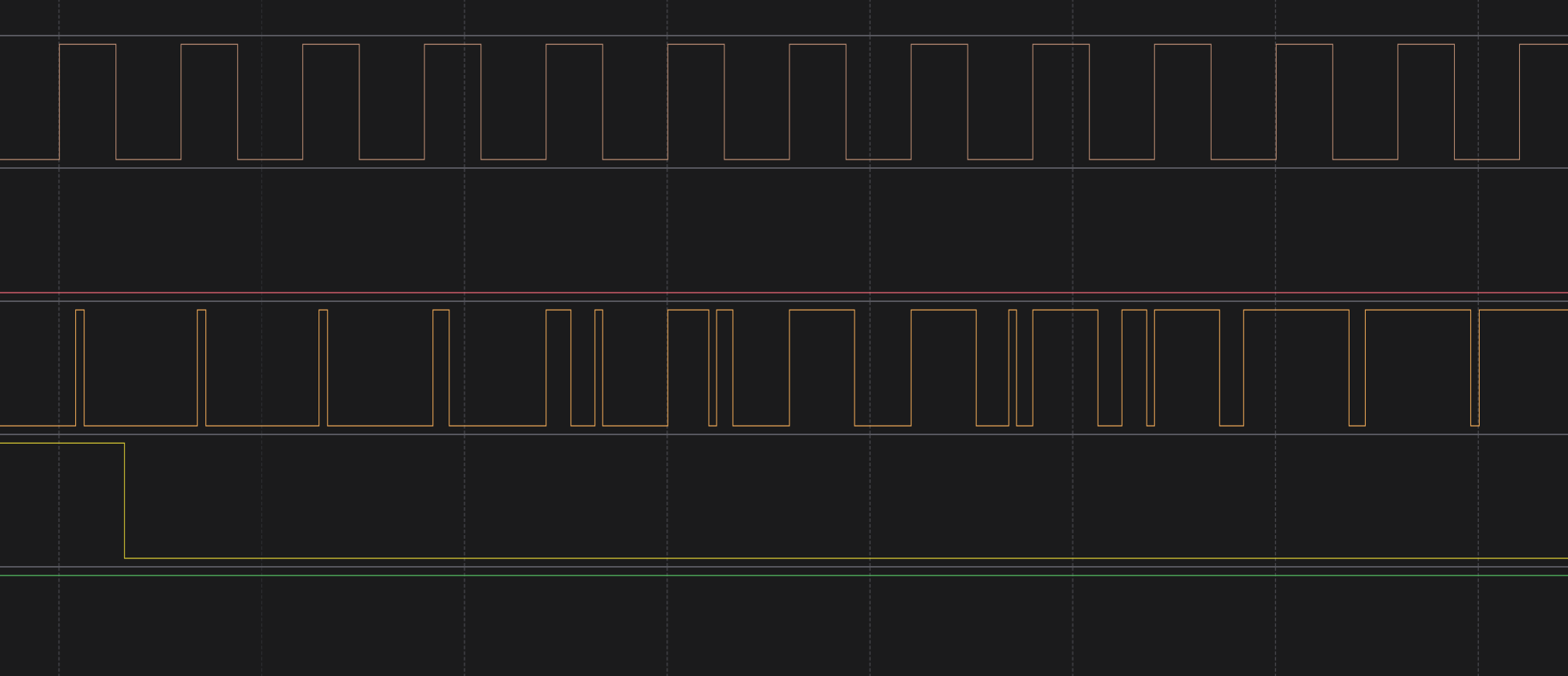
A few things immediately stand out when we zoom in on this region. First of all, it appears to be somewhat periodic, almost aligning with the presumed clock line in some places. More importantly, we have small pulses that are narrower than a single period of our clock! If these pulses were genuine, there is no way that they could be sampled at the examined clock speed!
Let's put the Saleae SPI analyzer on these signals and see what the results are:
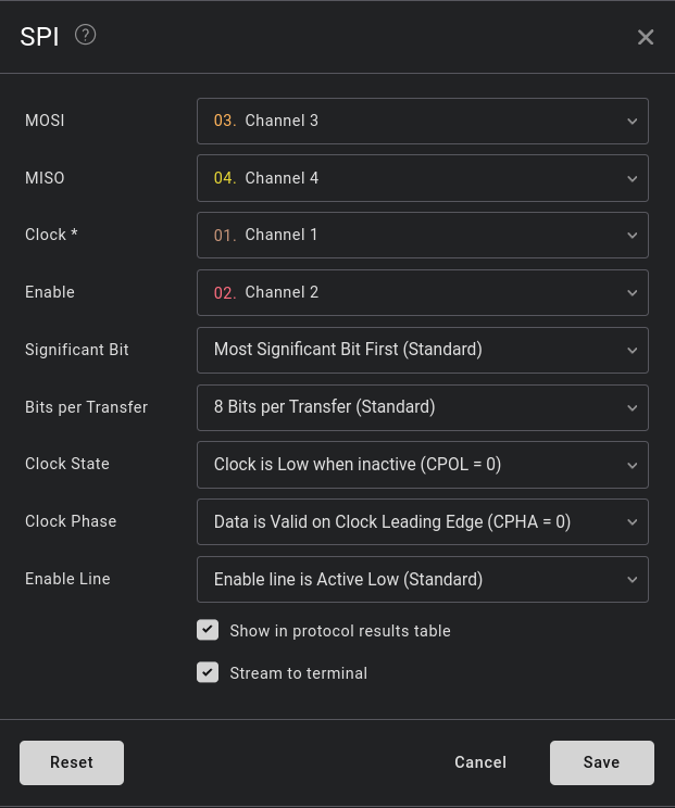
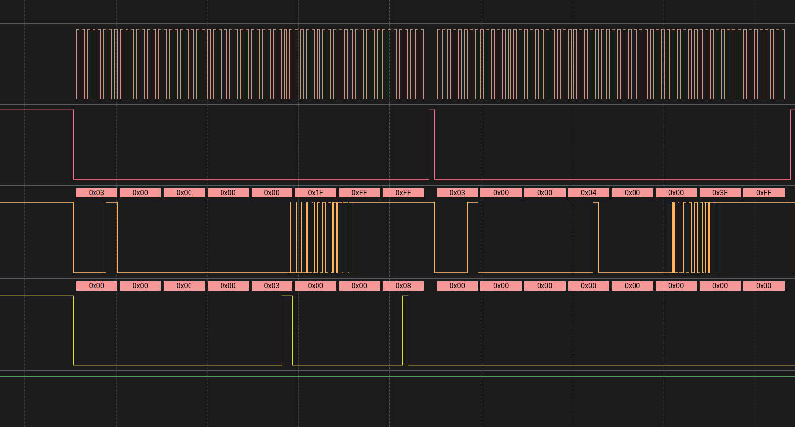
We can see in the above image that the traffic has been decoded, but what exactly does this mean? Does this noisy region present anything of value, or did we just cheap out on the jumper wires? To answer these questions we can take a look at the commands listed in the datasheet for our target SPI device; the core ones have been listed below:
| Opcode | Name |
|---|---|
0x9F |
JEDEC_ID (Read ID) |
0x03 |
READ |
0x0B |
FAST_READ |
0x6B |
FAST_READ_QUAD_OUT |
0x05 |
RDSR1 (Read Status Register-1) |
0x06 / 0x02 |
WREN / PAGE_PROGRAM |
0x20 |
SECTOR_ERASE (4 KiB) |
0xD8 |
BLOCK_ERASE (64 KiB) |
The first byte on D3 is 0x03, so it looks like this might be a read command. We can look in the datasheet to learn more about how this command is structured:
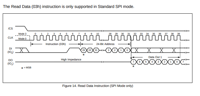
The WaveDrom diagram below shows the structure of a READ transaction:
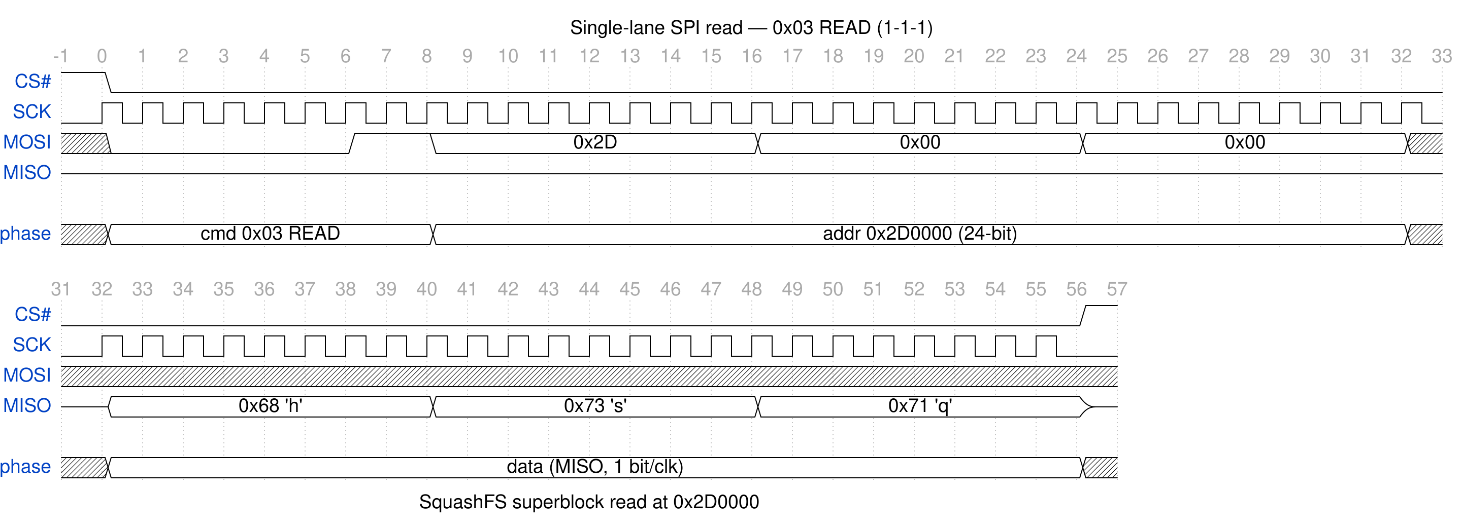
Armed with this information, if we look at our capture it starts to make a little more sense:
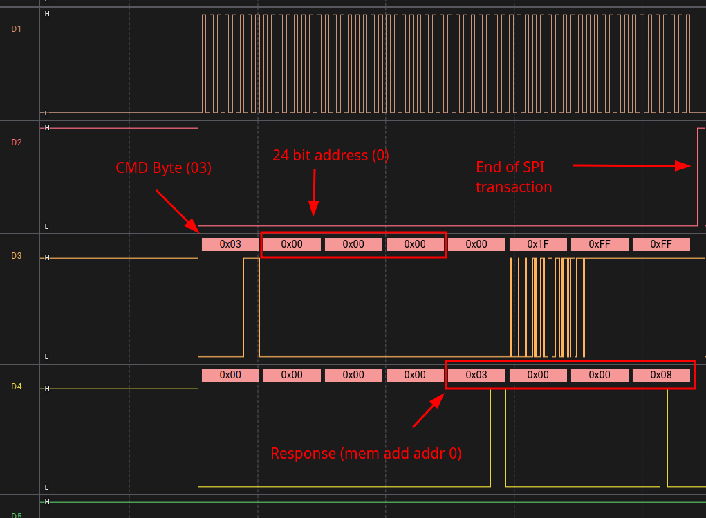
We can see that we have a read at address 0, and the response bytes are 03 00 00 08 (or 0x08000003 if you read them as a little-endian 32-bit word). Note that the 0x1F and 0xFF values that we see on D3 are during a time period where we "don't care" what comes over that line, indicated by the hatched regions in the timing diagram.
So within this transaction we have the target address, and the data at that address. We also have the length of the read, which is delimited by the CS line going high.
Now that we know how to interpret a single transaction, we can export all of the decoded bytes in the capture to a CSV file. This gives us every byte sent on DI/DO, which we can then parse.
The exported results look like this:
name,type,start_time,duration,"mosi","miso"
...
"SPI","enable",0.849574428,0.000000004,,
"SPI","result",0.84957446,0.000000452,0x03,0x00
"SPI","result",0.84957494,0.000000452,0x00,0x00
"SPI","result",0.84957542,0.000000452,0x01,0x00
"SPI","result",0.8495759,0.000000452,0x3C,0x00
"SPI","result",0.84957638,0.000000452,0x00,0x04
"SPI","result",0.84957686,0.000000452,0x00,0x00
"SPI","result",0.84957734,0.000000452,0xFF,0x29
"SPI","result",0.84957782,0.000000452,0xFF,0x25
"SPI","disable",0.849578332,0.000000004,,
Notice that the exporter denotes enable, disable and result rows. This is extremely useful, as we can use these to split up individual SPI transactions!
In the next section, we'll talk about extending Scapy to parse and understand these packet structures.
A Quick Scapy Primer
Scapy describes a protocol as a Packet subclass with a fields_desc list. Each entry is a field - a typed, named slice of bytes that knows how to dissect itself from a buffer and build itself back into one. Packets stack into layers with the / operator, and bind_layers() tells Scapy how to pick the next layer automatically during dissection. Layers are an extremely powerful feature in Scapy, and the automotive protocols that they have developed demonstrate how these work very well!
For our initial analysis, we'll use the following fields for decoding our SPI traffic:
ByteEnumField- a one-byte field with a value-to-name dictionary, so0x03shows up asREADwhen you print it.ThreeBytesField- a 24-bit integer, the width of a SPI flash address.ConditionalField- wraps another field and only includes it when a predicate is true. This is helpful for commands that take an address or require additional parsing.FieldLenField/StrLenField- a length field paired with a variable-length byte field, for payloads whose size we know.FlagsField- a bitfield with named bits, very helpful for something like a status register.
Modeling SPI Flash in Scapy
We'll define three layers:
- A thin
SPIbase layer that just records which chip-select line a transaction belongs to (handy if you ever capture a bus with multiple devices on it). - An
SPIFlashCmdlayer for the request - opcode, optional address, optional dummy byte. - Response layers for the data that comes back - plain read data, and a decoded status register.
from scapy.packet import Packet, bind_layers
from scapy.fields import (
    ByteEnumField, ByteField, ThreeBytesField,
    ConditionalField, FieldLenField, StrLenField, FlagsField,
)


class SPI(Packet):
    """Base layer — which chip-select line did this transaction belong to."""
    name = "SPI"
    fields_desc = [
        ByteEnumField("cs", 0, {0: "flash"}),   # add more CS lines as needed
    ]


class SPIFlashCmd(Packet):
    """A single SPI NOR flash command (the MOSI side of a transaction)."""
    name = "SPIFlashCmd"

    COMMANDS = {
        0x03: "READ",
        0x0B: "FAST_READ",
        0x6B: "FAST_READ_QUAD_OUT",   # 1-1-4: opcode + addr on IO0, data on IO0-IO3
        0x02: "PAGE_PROGRAM",
        0x05: "RDSR1",
        0x35: "RDSR2",
        0x06: "WREN",
        0x04: "WRDI",
        0x20: "SECTOR_ERASE",
        0xD8: "BLOCK_ERASE",
        0x9F: "JEDEC_ID",
    }

    CMD_READ      = 0x03
    CMD_FAST_READ = 0x0B
    CMD_RDSR1     = 0x05

    # Commands that clock out a 24-bit address after the opcode
    CMD_HAS_ADDR  = {0x03, 0x0B, 0x6B, 0x02, 0x20, 0xD8}
    # ...and of those, only the FAST_READ variants insert dummy cycles before data
    CMD_HAS_DUMMY = {0x0B, 0x6B}

    fields_desc = [
        ByteEnumField("cmd", CMD_READ, COMMANDS),
        ConditionalField(
            ThreeBytesField("addr", 0),
            lambda p: p.cmd in p.CMD_HAS_ADDR,
        ),
        ConditionalField(
            ByteField("dummy", 0),
            lambda p: p.cmd in p.CMD_HAS_DUMMY,
        ),
    ]


bind_layers(SPI, SPIFlashCmd, cs=0)
Notice how the READ vs FAST_READ distinction collapses into two small sets and a ConditionalField. The address is present for {0x03, 0x0B, 0x6B, 0x02, 0x20, 0xD8}; the dummy byte is present only for the fast reads (0x0B, 0x6B). Scapy now builds and dissects the right header for any of these commands with no special-casing in our parsing code.
The full spidump model goes one step further and uses a MultipleTypeField to switch the address between 24 and 32 bits for the 4-byte-address read opcodes, but the 24-bit version above is all we need for this chip.
For the data that comes back, a read response is just a length-prefixed blob:
class SPIFlashReadResp(Packet):
    name = "SPIFlashReadResp"
    fields_desc = [
        FieldLenField("dlen", None, length_of="data", fmt="I"),
        StrLenField("data", b"", length_from=lambda p: p.dlen),
    ]
Quick Detour: We've mostly been focusing on SPI flash reads for obvious reasons, but we can extend Scapy to help us analyze other commands, like the 0x05 read status register (RDSR1) command. When this command is issued, the flash chip responds with its current status. It is often used during erase and reprogramming operations to determine when the chip is done writing or erasing a page. As an example of how to use the FlagsField, we can parse out the individual bits of the status register whenever it is seen on the bus:
class SPIFlashStatusResp(Packet):
    name = "SPIFlashStatusResp"
    fields_desc = [
        FlagsField("sr", 0, 8, {
            0x01: "BUSY",   # erase/write in progress
            0x02: "WEL",    # write enable latch
            0x04: "BP0",
            0x08: "BP1",
            0x10: "BP2",
            0x20: "TB",     # top/bottom protect
            0x40: "SEC",    # sector protect
            0x80: "SRP0",   # status register protect 0
        })
    ]
Now a status byte of 0x02 dissects to <SPIFlashStatusResp sr=WEL> instead of a magic number. That readability is the whole point of pushing the protocol into Scapy.
Capture to Bytes
In the CSV that we exported from Saleae, there are three row types:
enable→CS#went low; a transaction is starting.result→ one byte was clocked; themosiandmisocolumns hold the two sides.disable→CS#went high; the transaction is complete.
So a transaction is everything between an enable and the next disable. Our first step is to parse out these individual transactions; once we have the raw bytes, we can apply our decoder:
import csv

def parse_transactions(path):
    """Yield {'mosi': bytes, 'miso': bytes} for each CS-framed transaction."""
    current = None
    with open(path, newline="") as f:
        for row in csv.DictReader(f):
            ttype = (row["type"] or "").strip('"')

            if ttype == "enable":
                current = {"mosi": bytearray(), "miso": bytearray()}

            elif ttype == "result" and current is not None:
                mosi = row["mosi"] or ""
                miso = row["miso"] or ""
                current["mosi"].append(int(mosi, 16) if mosi.startswith("0x") else 0)
                current["miso"].append(int(miso, 16) if miso.startswith("0x") else 0)

            elif ttype == "disable" and current is not None:
                if current["mosi"]:
                    yield {"mosi": bytes(current["mosi"]),
                           "miso": bytes(current["miso"])}
                current = None
We don't need to pick the MOSI bytes apart by hand; we can hand them straight to SPIFlashCmd and let the ConditionalFields decide whether an address and dummy byte are present. Here is the first READ from our capture, the same transaction we annotated earlier:
>>> SPIFlashCmd(bytes.fromhex("03000000001fffff")).show()
###[ SPIFlashCmd ]###
  cmd       = READ
  addr      = 0
###[ Raw ]###
     load      = b'\x00\x1f\xff\xff'
Scapy pulled out the opcode and the 24-bit address, and everything the controller clocked out after the header - the "don't care" bytes, including the 0x1F and 0xFF values we saw on D3 - landed in a Raw payload. The length of the dissected header tells us exactly where the read data starts on MISO:
import struct

def transaction_to_packets(tx):
    mosi, miso = tx["mosi"], tx["miso"]

    # Let Scapy split the MOSI bytes into opcode / address / dummy.
    try:
        req = SPIFlashCmd(mosi)
    except struct.error:
        return None, None                # CS# went high mid-header
    hdr_len = len(req.self_build())      # opcode + addr + dummy, per the model

    pkt = SPI(cs=0) / req
    resp = None

    if req.cmd in (SPIFlashCmd.CMD_READ, SPIFlashCmd.CMD_FAST_READ):
        data = miso[hdr_len:]            # flash data lives on MISO
        if data:
            resp = SPIFlashReadResp(data=data)
    elif req.cmd == SPIFlashCmd.CMD_RDSR1 and len(miso) > hdr_len:
        resp = SPIFlashStatusResp(sr=miso[hdr_len])

    return pkt, resp
In the above example, we handle the READ, FAST_READ and RDSR1 commands. If we provide the exported CSV and parse some of the packets, we see the following:
>>> tx = next(t for t in parse_transactions("bigger-boot.csv")
...           if t["mosi"][0] == 0x05)
>>> pkt, resp = transaction_to_packets(tx)
>>> pkt.show()
###[ SPI ]###
  cs        = flash
###[ SPIFlashCmd ]###
     cmd       = RDSR1
###[ Raw ]###
        load      = b'\xff'

>>> resp.show()
###[ SPIFlashStatusResp ]###
  sr        = BP0+TB
Here we are just looking for status register requests via the RDSR1 command. We found one in the capture, and Scapy turns that bitfield into human-readable output! This is really helpful when reverse engineering a reflash sequence or an update protocol - and as it turns out, our capture contains one!
Catching the Device Writing to Flash
While going through the capture, we noticed that it wasn't just reads: there were over 2,000 PAGE_PROGRAM commands and a BLOCK_ERASE (0xD8, which we added to our model above) in the middle of the boot process. To make sense of these, we can write a small helper that turns each transaction into a one-line description and collapses repeated lines, since a flash chip gets polled a lot while it's busy:
from itertools import groupby

def describe(pkt, resp):
    cmd = pkt[SPIFlashCmd]
    line = cmd.sprintf("%cmd%")
    if cmd.cmd in SPIFlashCmd.CMD_HAS_ADDR:
        line += f" addr=0x{cmd.addr:06x}"
    if cmd.cmd == 0x02:                  # PAGE_PROGRAM: write data rides on MOSI
        line += f" ({len(cmd.payload)} bytes)"
    if isinstance(resp, SPIFlashStatusResp):
        line += " sr=" + resp.sprintf("%sr%")
    return line

def trace(txs):
    lines = (describe(*transaction_to_packets(tx)) for tx in txs)
    for line, group in groupby(lines):
        n = sum(1 for _ in group)
        print(line if n == 1 else f"{line}  (x{n:,})")
Scapy's sprintf does most of the formatting work here: %cmd% renders the opcode through our ByteEnumField dictionary, and %sr% renders the status byte through the FlagsField bit names. For a page program, the data being written is clocked out on MOSI right after the address, so it ends up in the Raw payload of our SPIFlashCmd layer - here we just print its length.
Let's find the erase and trace from just before it up to the first page program:
>>> txs = list(parse_transactions("bigger-boot.csv"))
>>> erase = next(i for i, tx in enumerate(txs) if tx["mosi"][0] == 0xD8)
>>> pp = [i for i, tx in enumerate(txs) if tx["mosi"][0] == 0x02]
>>> trace(txs[erase - 3 : pp[0] + 1])
RDSR1 sr=BP0+TB
WREN
RDSR1 sr=WEL+BP0+TB
BLOCK_ERASE addr=0x730000
RDSR1 sr=BUSY+WEL+BP0+TB  (x210,836)
RDSR1 sr=BUSY+BP0+TB  (x2)
RDSR1 sr=BP0+TB  (x2)
WREN
RDSR1 sr=WEL+BP0+TB
PAGE_PROGRAM addr=0x730000 (32 bytes)
This is an erase and program sequence, with the order of operations taken straight from the datasheet!
RDSR1returnsBP0+TB- the chip is idle. The block protect bits are set, but withTBset they only protect the bottom 256 KiB of the flash, not the region being erased.WRENsets the Write Enable Latch, and the next poll showsWEL.BLOCK_ERASEwipes the 64 KiB block at0x730000, andBUSYgoes high.- The controller polls the status register over 210,000 times until
BUSYclears WELclears automatically once the erase finishes, so the controller issues anotherWRENbefore it can program.
Each page program then follows the same pattern:
>>> trace(txs[pp[0] - 2 : pp[1] - 2])
WREN
RDSR1 sr=WEL+BP0+TB
PAGE_PROGRAM addr=0x730000 (32 bytes)
RDSR1 sr=BUSY+WEL+BP0+TB  (x47)
RDSR1 sr=BUSY+BP0+TB  (x2)
RDSR1 sr=BP0+TB
The device repeats this 2,048 times, 32 bytes at a time, from 0x730000 to 0x73ffe0 - rewriting the entire 64 KiB block that it just erased, and taking a little over 400 ms of the boot to do it. On this device, that block holds the device's configuration, which is exactly the kind of thing you want to take note of during an assessment.,
Note: Our reconstruct function below only replays reads, so data written with PAGE_PROGRAM does not show up in the recovered image. If you want to see what the device wrote, those bytes are sitting in the Raw payload of each PAGE_PROGRAM packet.
Next, let's move on to what we really want to do: reconstructing the flash image.
Reconstructing the Flash Image
With our Scapy definitions, every READ transaction tells us that, at some address, the flash held these bytes. By collecting all of these reads, we can reconstruct a flash image based on what the CPU requested during boot.
Note: The default state of an erased NOR flash is 0xFF, so we will initialize our image with all 0xFFs and then fill in the captured offsets with the data captured at that address.
def reconstruct(path, flash_size=0x1000000, fill=0xFF):
    image = bytearray([fill]) * flash_size
    coverage = bytearray(flash_size)          # 1 where we have real data

    for tx in parse_transactions(path):
        pkt, resp = transaction_to_packets(tx)
        if not isinstance(resp, SPIFlashReadResp):
            continue

        addr = pkt[SPIFlashCmd].addr
        data = resp.data
        end = min(addr + len(data), flash_size)

        image[addr:end] = data[:end - addr]
        coverage[addr:end] = b"\x01" * (end - addr)

    covered = sum(coverage)
    pct = 100 * covered / flash_size
    print(f"reconstructed {covered:,} / {flash_size:,} bytes ({pct:.1f}%)")
    return bytes(image), coverage


image, coverage = reconstruct("bigger-boot.csv")
with open("recovered_flash.bin", "wb") as f:
    f.write(image)
Reconstruction in Practice
After running this script on our capture, we were able to reconstruct the bootloader and kernel image; however, there was no root filesystem!
[wrongbaud@mechanicus extractions]$ binwalk recovered_flash.bin
--------------------------------------------------------------------------------------------------------------------------------
DECIMAL                            HEXADECIMAL                        DESCRIPTION
--------------------------------------------------------------------------------------------------------------------------------
39192                              0x9918                             CRC32 polynomial table, little endian
40288                              0x9D60                             gzip compressed data, operating system: Unix, timestamp: 2021-04-28 08:49:30, total size: 47275 bytes
337944                             0x52818                            LZMA compressed data, properties: 0x5D, dictionary size: 8388608 bytes, compressed size: 2325913 bytes, uncompressed size: 7676180 bytes
If you've looked at embedded firmware before, this likely looks very familiar. Reviewing the strings shows us the following:
Booting...
init_ram
init ddr ok
DRAM Type: DDR2
        DRAM frequency: %dMHz
        DRAM Size: %dMB
333333333333
ffffffffDT
DDDDDDDDD
Detect page_size = 2KB (%d)
Detect bank_size = 8 banks(0x%x)
Detect dram size = 128MB (0x%x)
bond:0x%x
MCM 128MB
DDR init OK
 %s ,ddr_freq=%d (Mbps), %d (MHZ)
DRAM init disable
DRAM init enable
DRAM init is done , jump to DRAM
enable DRAM ODT
SDR init done dev_map=0x%x
dram_init_clk_frequency
This looks like early bootloader code (DRAM initialization), which makes sense given that we were capturing on boot. This still leaves one question - where is our root filesystem?
There are two likely explanations:
- We didn't capture a full boot sequence.
- The SPI flash is being re-enumerated in QSPI mode.
Let's talk a bit more about QSPI before we dig into these captures.
QSPI Analysis
While we've covered standard single-lane SPI in our write-ups before, we've not had the chance to talk about Quad-SPI, or QSPI. Quad SPI (as the name implies) allows for faster data read speeds by outputting data in parallel across IO0-IO3. Let's review our pinout one more time:
In single-lane mode, only two pins move data: DI (IO0) and DO (IO1). The other two - /WP (IO2) and /HOLD or /RESET (IO3) - are static control lines. In quad mode, all four become bidirectional data lines, so the opcode, address, and/or data get clocked out a nibble at a time across IO0–IO3 instead of one bit on a single line. The definitive tell that you're in quad mode isn't just a faster clock, it's that the former /WP and /HOLD pins suddenly start carrying traffic.
An example of what a QSPI flash read looks like can be seen in the WaveDrom diagram below:
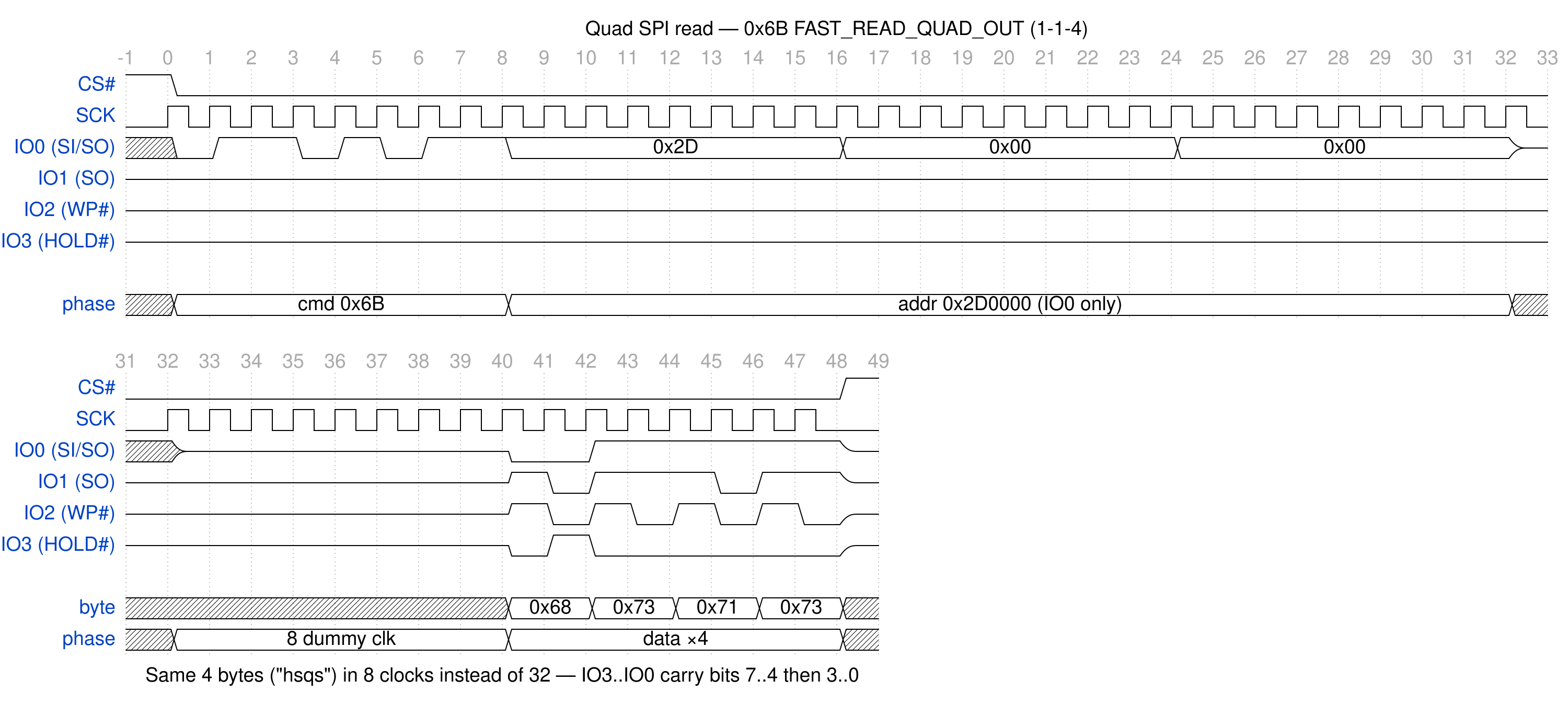
To check for this, we can take a longer capture and examine the state of the data lines. If activity suddenly appears on /WP and /HOLD, then we know that the device is transitioning to QSPI mode. Sure enough, after taking a longer capture we saw those lines become active, along with another tell. Let's look at our clock line at the beginning and end of the capture:
Standard SPI, ~16 MHz:
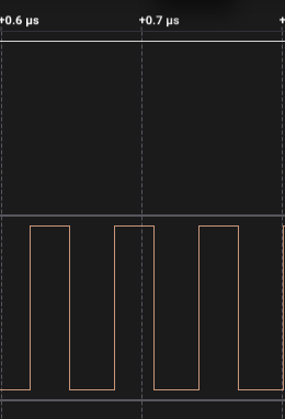
After the switch, ~50 MHz:
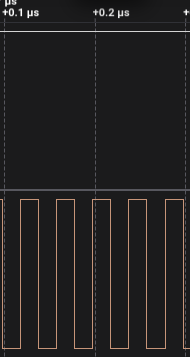
At the same time scale, there are roughly three times as many clock edges - and with four data lanes instead of one, read throughput goes up by about 12x. The kernel has reconfigured the flash controller and switched into Quad SPI (QSPI) mode, cranking the clock and widening the data path.
The read command used after the switch is 0x6B (Fast Read Quad Output), which is a 1-1-4 command: the opcode and address are still clocked out on IO0 alone, then 8 dummy clocks, and only the data phase uses all four lanes. You can see this in the Lines Used column of the export below.
This switch is a problem for us! The default SPI analyzer in Saleae does not support QSPI mode, so we will need to use an additional analyzer and break up this capture into two sessions: one for single-lane SPI, and one for QSPI. Luckily for us, the QSPI-Analyzer plugin for Saleae Logic / KingstVIS does exactly that. We point it at all four IO channels plus CLK and CS, tell it the lane widths and dummy-cycle count for the command in use, and let it decode each transaction.
There is only one small issue, though: when we export the QSPI capture, we now have this table:
Time [s],Packet ID, Transaction State, DATA, Lines Used
8.196254324,0,1,0x6B,1        <- state 1: command  (1 line)
8.196254486,0,2,0x380000,1    <- state 2: address  (1 line)
8.196254970,0,3,Dummy,1       <- state 3: dummy cycles
8.196255131,0,4,0x85,4        <- state 4: data byte (4 lines)
8.196255172,0,4,0x19,4
...
That's a different shape from the single-lane enable/result/disable table - the analyzer has already split each transaction into command / address / dummy / data states, with a Lines Used column recording the lane width. Our tool, spidump, auto-detects this header and walks the state machine, but everything downstream is unchanged: each transaction still becomes a SPIFlashCmd (0x6B is just another read opcode in the model) and feeds the same reconstruct routine - because Scapy models the logical transaction, not the number of wires it came in on.
Pointing the extended tool at the quad capture rebuilds everything the device read after the switch:
$ python main.py big-quad-spi-analyzed-dump.txt -o quad.bin -v
detected capture format: qspi-analyzer
commands seen: {'FAST_READ_QUAD_OUT': 36839, 'RDSR1': 25674}
flash_size=0x1000000  read_txns=36839  covered=11288528 (67.3%)
wrote 16777216 bytes -> quad.bin

$ binwalk quad.bin
DECIMAL     HEXADECIMAL   DESCRIPTION
--------------------------------------------------------------------------
2949120     0x2D0000                           SquashFS file system, little endian, version: 4.0, compression: xz, inode count: 734, block size: 131072, image size: 3157356 bytes, created: 2038-02-22 09:50:56
14548992    0xDE0000                           JFFS2 filesystem, little endian, nodes: 523, total size: 2031628
But notice what's missing: binwalk finds nothing below 0x2D0000, because everything in that region is 0xFF. That's not empty flash - it's the bootloader and kernel, which the device read in single-lane mode before it ever switched to quad. The quad capture starts after the switch, so they aren't in it. This time we have the rootfs, but we're missing the bootloader and kernel. Since our single-lane capture already gave us those, we can merge the two images together to get a very decent-looking firmware image! A quick way to do this is with dd, copying everything from 0x2D0000 up out of the quad image and into the single-lane image:
dd if=quad.bin of=recovered_flash.bin bs=64K iflag=skip_bytes oflag=seek_bytes \
   skip=$((0x2D0000)) seek=$((0x2D0000)) conv=notrunc
spidump can also do this for you with --merge, which layers the reads from multiple captures on top of each other and drops any reads that were decoded at the wrong lane width (for example, quad reads that the single-lane analyzer mis-decoded):
python main.py bigger-boot.csv --merge big-quad-spi-analyzed-dump.txt -o recovered_flash.bin -v
Either way, binwalk now shows the full picture:
[wrongbaud@mechanicus extractions]$ binwalk recovered_flash.bin
-------------------------------------------------------------------------------------------------------------------------------------------
DECIMAL                            HEXADECIMAL                        DESCRIPTION
-------------------------------------------------------------------------------------------------------------------------------------------
39192                              0x9918                             CRC32 polynomial table, little endian
40288                              0x9D60                             gzip compressed data, operating system: Unix, timestamp: 2021-04-28 08:49:30, total size: 47275 bytes
337944                             0x52818                            LZMA compressed data, properties: 0x5D, dictionary size: 8388608 bytes, compressed size: 2325913 bytes, uncompressed size: 7676180 bytes
2949120                            0x2D0000                           SquashFS file system, little endian, version: 4.0, compression: xz, inode count: 734, block size: 131072, image size: 3157356 bytes, created: 2038-02-22 09:50:56
14548992                           0xDE0000                           JFFS2 filesystem, little endian, nodes: 523, total size: 2031628 bytes
-------------------------------------------------------------------------------------------------------------------------------------------
Now for the final test: can we extract this SquashFS image and find any reasonable data?
[wrongbaud@mechanicus results]$ dd if=recovered_flash.bin of=squashfs2.bin bs=1 skip=$((0x2D0000)) count=3157356
3157356+0 records in
3157356+0 records out
3157356 bytes (3.2 MB, 3.0 MiB) copied, 2.1317 s, 1.5 MB/s
[wrongbaud@mechanicus results]$ file squashfs2.bin
squashfs2.bin: Squashfs filesystem, little endian, version 4.0, xz compressed, 3157356 bytes, 734 inodes, blocksize: 131072 bytes, created: Mon Feb 22 09:50:56 2038
[wrongbaud@mechanicus results]$ unsquashfs squashfs2.bin
Parallel unsquashfs: Using 24 processors
703 inodes (291 blocks) to write
created 238 files
created 31 directories
created 116 symlinks
created 0 devices
created 0 fifos
created 0 sockets
created 0 hardlinks
[wrongbaud@mechanicus squashfs-root]$ ls
bin  dev  etc  home  include  init  lib  mnt  proc  root  sbin  sys  tmp  usr  var  web
Nice! We were able to extract the SquashFS from nothing but SPI captures. Now the real work can begin!
Conclusion
With this post, we've demonstrated how to reconstruct a firmware image from a SPI traffic capture. This tooling supports both standard and quad SPI and allows flash contents to be reconstructed without removing the target flash device. There are, of course, some drawbacks: we can only reconstruct what the device reads while we're watching, but for the purposes of initial reverse engineering and triage, this is a great starting point.
This tooling can also be used to analyze and review SPI traffic from devices other than NOR flash, allowing for increased introspection when reverse engineering custom protocols.
All relevant tooling can be found here.
Keep an eye out for our next post, where we extend this to I2C and develop another Scapy plugin!
Happy Hacking!
Matt (wrongbaud)
Contact / Training
If you're looking to learn more about hardware reverse engineering, check out our roadmap of free resources here. If you're interested in structured training for your team, check out our hardware hacking bootcamp. And if you'd like an in-depth dive into how hardware-level debuggers work and how to reverse engineer them, check out our self-paced course here.
Note: We are launching a new variant of the Hacking Hardware Debuggers course in Q4, which will be significantly cheaper and will not come with a pre-configured hardware kit. Students will get access to all of the relevant tools and a list of hardware to purchase if they wish to follow along.
If you want to stay informed about official releases, new courses, and blog posts, sign up for our mailing list here.
Lastly, if you want to secure your devices/firmware with an audit from us, please don't hesitate to reach out to contact@voidstarsec.com.