Brushing Up on Hardware Hacking Part 2 - SPI, UART, Pulseview, and Flashrom
Overview
In our last post, we reviewed how to use the pi-gen tool to generate an image for a Raspberry Pi that is pre-configured with many tools needed for basic hardware hacking. In this post, we will start using them on our first target.
Our first target from the AliExpress grab bag is going to be this electric toothbrush. Our goal is to extract the firmware and maybe push modified firmware to the toothbrush (there is a statement I never thought I'd type...).
This toothbrush is an interesting target for several reasons:
- It has a (somewhat) high-res color screen
- This leads me to believe that whatever is driving it might be somewhat interesting
- It has a USB port
- This might be used just for charging, but there is only one way to find out
- There are user presets as well as a "version" screen
- This might mean some non-volatile storage on board and, more importantly, a firmware update method!
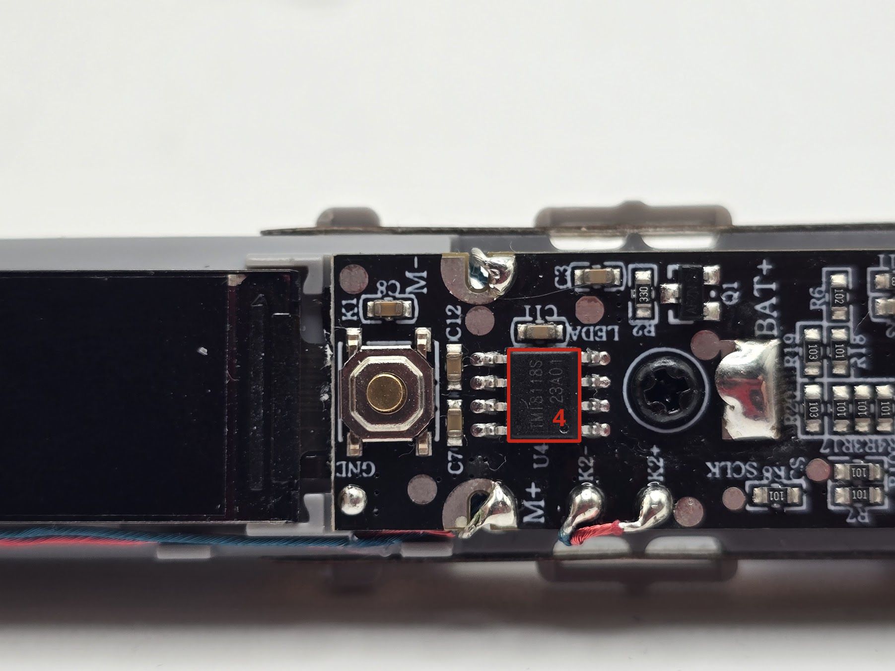
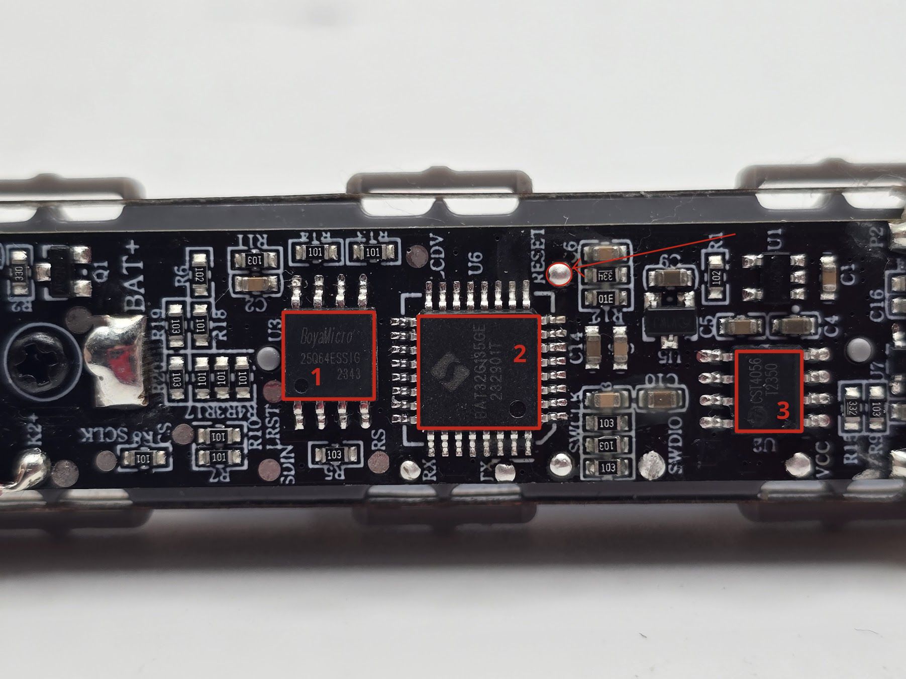
One of the first things we want to do with a new embedded target is perform a visual teardown. During this process, we will identify the various components and potential attack vectors (exposed pins/pads) that we will use to extract information from this device. The visual teardown for this device can be seen in the image/tables below:
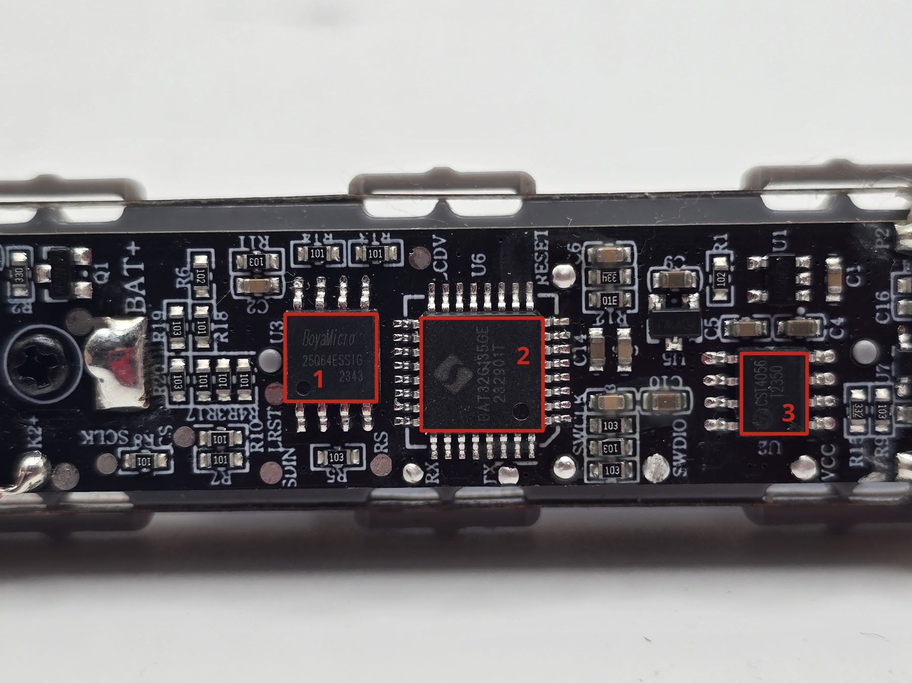
| Number | Part Number | Datasheet | Usage |
|---|---|---|---|
| 1 | BoyaMicro 25Q64ESSIG | Link | SPI Flash, non-volatile storage |
| 2 | BAT32G135 MCU | Website Overview, Datasheet | 32 bit ARM Cortex M0 MCU |
| 3 | CST4056 | Link | Standard Linear Li-Ion Battery Charger |
| 4 | TMI8118S | Link | Brushed DC Motor Driver |
This is a pretty simple target, which makes it great for learning how to do embedded assessments. We have an ARM Cortex MCU, an SPI flash, an IC for managing the charging of the battery, and another IC for controlling the motor. This target also contains a very well-documented silkscreen, which makes our initial analysis much simpler; one thing that likely stuck out to you when examining this PCB was the clearly labeled Tx and Rx pads, as we've discussed in previous posts this is indicative of a UART. Let's start by looking at this toothbrush's UART output.
Target 0: UART (?!)
If you've never looked at UART before or are unfamiliar with the process of identifying one and locating the baud rate, I highly recommend checking out the post I linked previously. It will cover everything you need to know for the following section.
The first thing we need to do is determine the baud rate; once we have that, we can look at the data being sent over the lines and determine if it is useful to us. Using an oscilloscope, we can monitor this line on startup, which results in the following trace being generated on the scope:
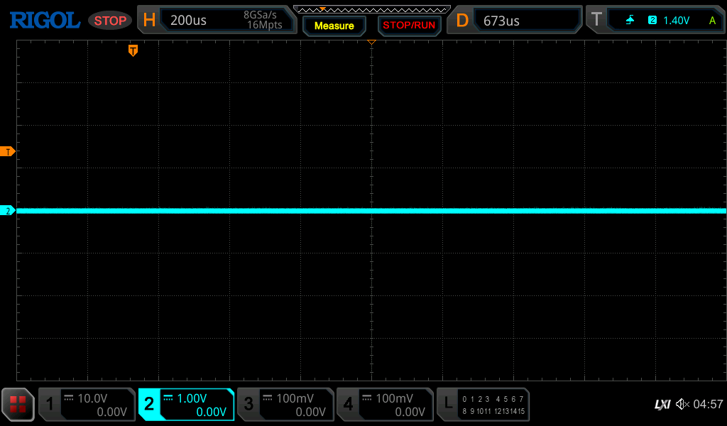
This does not look promising in terms of debug output. However, If you are familiar with UART, you know that the transmit line must be pulled high as bits are (in a standard configuration) transmitted by driving the line low. We can see in this capture that the line is low. This may lead you to think that the UART is not active and we should move on; before we do that, let's try one more thing. Using a 10K resistor, we will pull the Tx line high to 3.3V; if we take a capture in this configuration and press a few buttons on the toothbrush, we see the following:
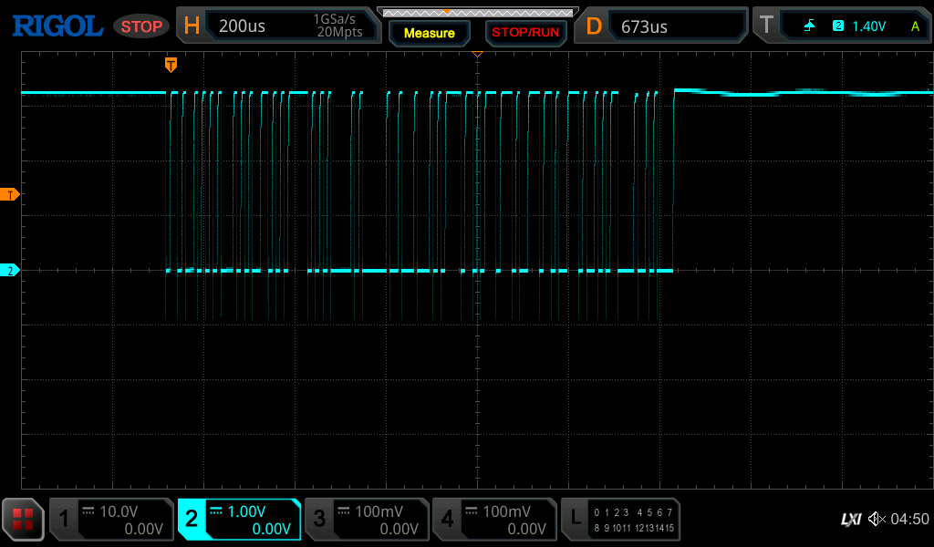
Success! We have traffic, so the lesson here is not to get discouraged if you don't immediately see traffic on a UART interface. It is important to rely on your understanding of the protocol fundamentals at a low level, this is something that we focus on at the core of our hardware reverse engineering training.
Based on the output from the scope, we determine that the baud rate is 115200; this is done by locating the smallest pulse and measuring its frequency. Now that we have this we can connect this to the serial port of the Raspberry Pi and examine the output:
KEY_B Down.
KEY_B Dn->Up.
KEY_B Down.
39F9(8000,9419),
KEY_B Dn->Up.
KEY_B Down.
KEY_B Dn->Up.
KEY_A Down.
675D(30000,33884),
4C91(10,3894), 675D(30000,33884),
So, we have debug output! But this does not get us what we're looking for. We want to extract the firmware and see if we can re-flash it! For these purposes, we will focus on the main MCU and the SPI flash. Let's start by looking at the SPI flash.
Target 1: SPI Flash
If you are unfamiliar with SPI flash chips and how they work, check out some of our previous blog entries here.
In order to read out this flash we will use flashrom. If you are unfamiliar with flashrom, it is an open-source tool for reading and writing SPI flash devices. We've used this tool in previous posts, and you can learn more about it and see more usage examples here
One of the nice things about flashrom is that we can use it with several hardware adapters. One of the most commonly used is the CH341 adapter, which you can purchase here. However, you can also use an embedded Linux device with the spidev kernel module loaded, allowing an SPI peripheral to be accessed through the /dev/ directory.
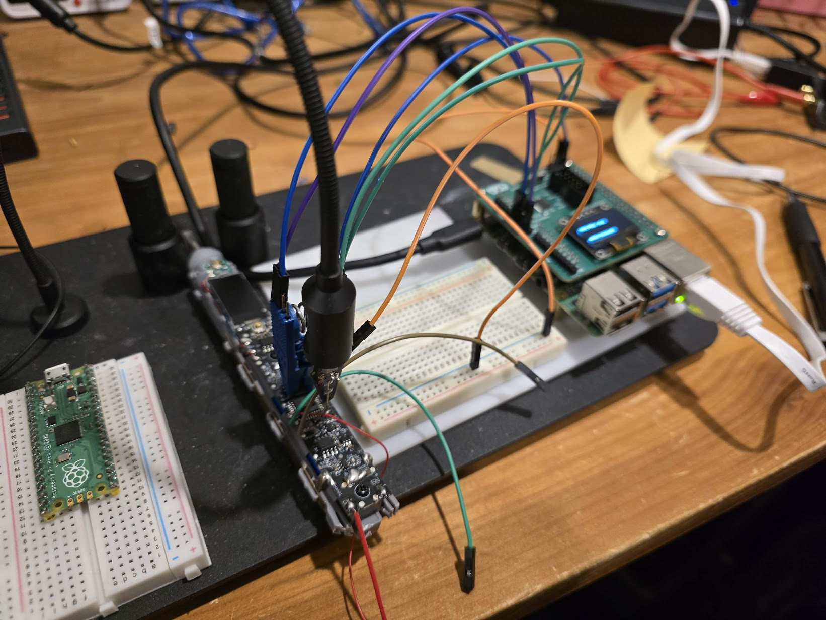
We can attempt to access the SPI flash using a standard SOIC8 clip (pomona are the best) as shown in the diagram:
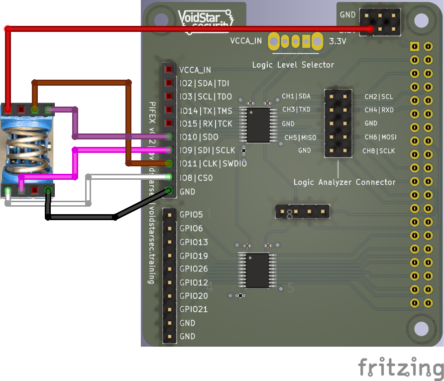
Running Flashrom
Using a Raspberry Pi with the spidev kernel module enabled, we can attempt to extract the SPI flash as follows:
sudo flashrom -p linux_spi:dev=/dev/spidev0.0 -r toothbrush-spi.bin
-pis used to specify the programmer; on our case this is the SPI peripheral on the Raspberry Pi (linux_spi) located at/dev/spidev0.0- Note: If you are using something like an FTDI, Tigard, or CH341 programmer, you will want to update this according to your hardware
-rspecifies a read operation followed by the filename that we want to write.
So, with our clip in place, we should be able to just run it and get access to the SPI data, right? Let's see what happens:
pi@pifex:~/targets/toothbrush $ ./run-flashrom.sh r spi.bin
flashrom unknown on Linux 6.6.74+rpt-rpi-v8 (aarch64)
flashrom is free software; get the source code at https://flashrom.org

Using clock_gettime for delay loops (clk_id: 1, resolution: 1ns).
Using default 2000kHz clock. Use 'spispeed' parameter to override.
No EEPROM/flash device found.
Note: flashrom can never write if the flash chip isn't found automatically.
If you have used flashrom before, errors like this are not new to you, if you have not, don't fret! Recall that one of the pins we connected to for the SPI flash was the VCC pin. If that pin is also connected to the CPU on board, then we are likely inadvertently powering this CPU and causing it to access the SPI flash while we are trying to read. This will cause bus contention problems as the SPI protocol cannot have two host devices actively trying to access the same target device simultaneously.
In this scenario, there are several options that we have:
- Remove the SPI flash with a hot air gun
- Pros: Immediately remove the bus contention issues
- Cons: Removal/resoldering the device can be risky if you've not done this before. If there is any type of anti-tamper on the target device, it may cause issues for us as well
- Analyze the SPI traffic using a logic analyzer and reconstruct the data that is read from the CPU to a flash image
- Pros: Non-invasive, can be done with Pulseview
- Cons: If the CPU does not address the entire SPI flash, we will not get a full image; also, depending on the system, adding the additional length to the SPI traces by attaching our logic analyzer can cause the CPU not to boot properly. This method also, by definition gives us no write access, so if we want to push modified firmware - we are out of luck
- Find a way to keep the CPU in reset or stop communicating with the SPI flash
- Pros: Allows for in-circuit reads
- Cons: Based on the PCB layout of your target and your level of access, this may not be possible
Let's go through all three of these together. For our first example, I have an old blog post here that walks through the process.
Analyzing Data with Pulseview
Using the same clip setup as before, we can use a low-cost logic analyzer to view the traffic on startup and during operations:
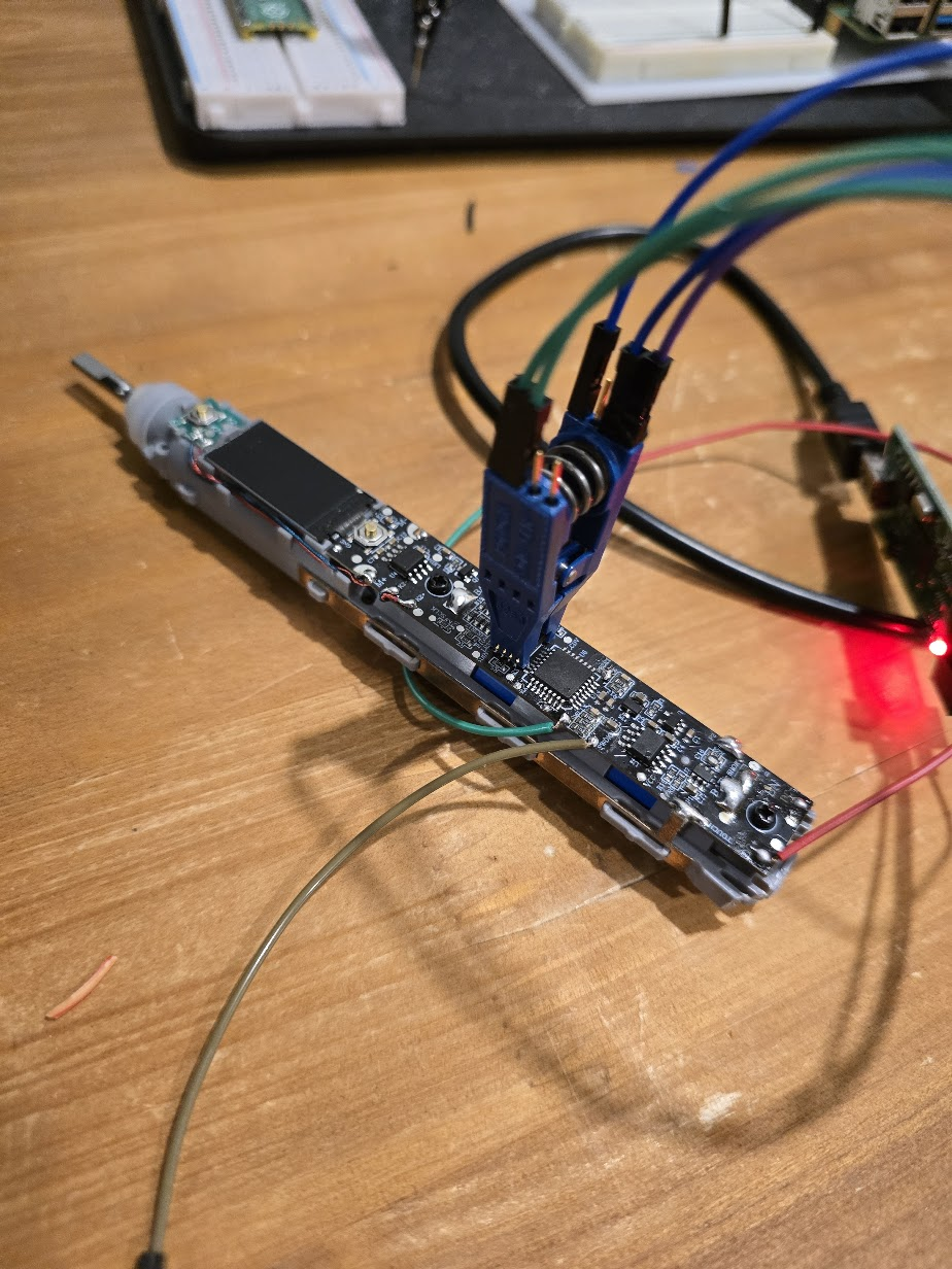
After monitoring the SPI traffic on boot, we have the following:
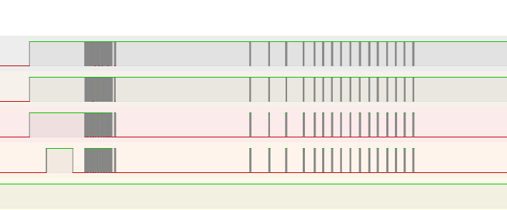
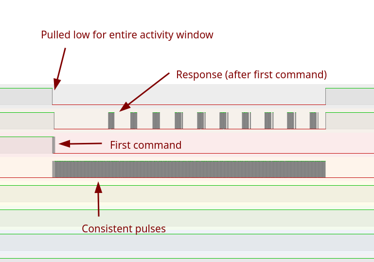
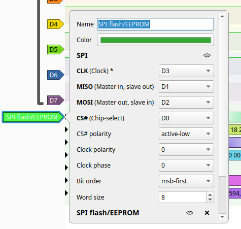
With this, we can set up an SPI decoder and assign the signals, as shown below. Pulseview also includes protocol-level decoders that we can use to see exactly what commands are being sent to this SPI flash.
While we know the pins we have connected to on the SPI flash, let's examine the traffic and see if we can identify them. This skill can be helpful if you are analyzing signals on an undocumented bus or debug header.
Note: If you would like more of a deep dive into the SPI protocol and how it is used for EEPROMs, check out my old blog post here
Serial Peripheral Interface (SPI) requires the following four signals:
- Chip Select: Used to select the target chip
- Clock: Driven by the host to determine when data is sampled
- Serial Data Out (MOSI): Data sent from the host to the target is sent on this line
- Serial Data In (MISO): Used to send data from the device to the host.
Based on what we know about the SPI protocol, the CS line should stay low during each transaction. This behavior is seen on the D0 line in our screenshot above. Next, we know that a clock signal has to be provided by the bus controller; this will be a consistent pulse that aligns with data being transmitted on the target. The fourth row in the screenshot above demonstrates this. Now, all that is left is the SDI and SDO lines. SDO is driven by the controller and used to issue commands; replies are then sent back to the SDI line.
If we look closely at our captured signals, we can see that one line is active first (3), which is followed by a response on the other line (2). It is a fair assumption to label the third signal as SDO and the second as SDI; we can set this up in our pulseview decoder as shown below:
With our decoder set up, we can see the bytes that are being sent and what those bytes mean to the SPI flash:
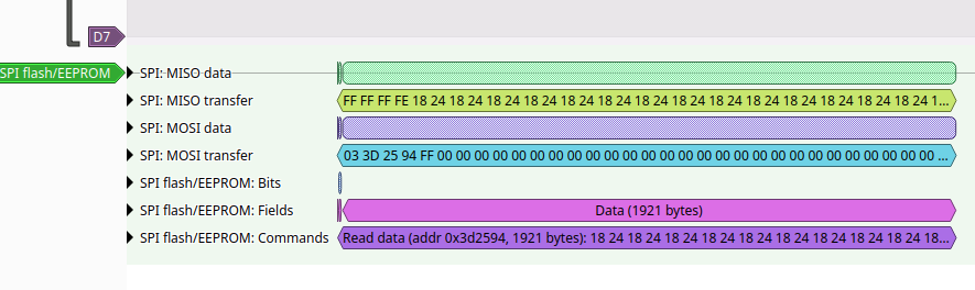
One thing to note is that when a read operation is performed (when cycling through the menus) and new data is displayed on screen, we have the following transactions:
- Thirteen read operations, each consisting of 1,921 bytes (24973 bytes total)
- One final read consisting of 641 bytes
It is a reasonable assumption to say that the data for each image displayed requires roughly 24Kb of data.
One of the most useful features in Pulseview is the "Binary Decoder Output View." This window will let you view decoded traffic results and export them to a file. In the following screenshot, we have selected the MISO (SDI) line, which shows the responses from the SPI flash. This contains the data that was transmitted back to the CPU from the flash chip.
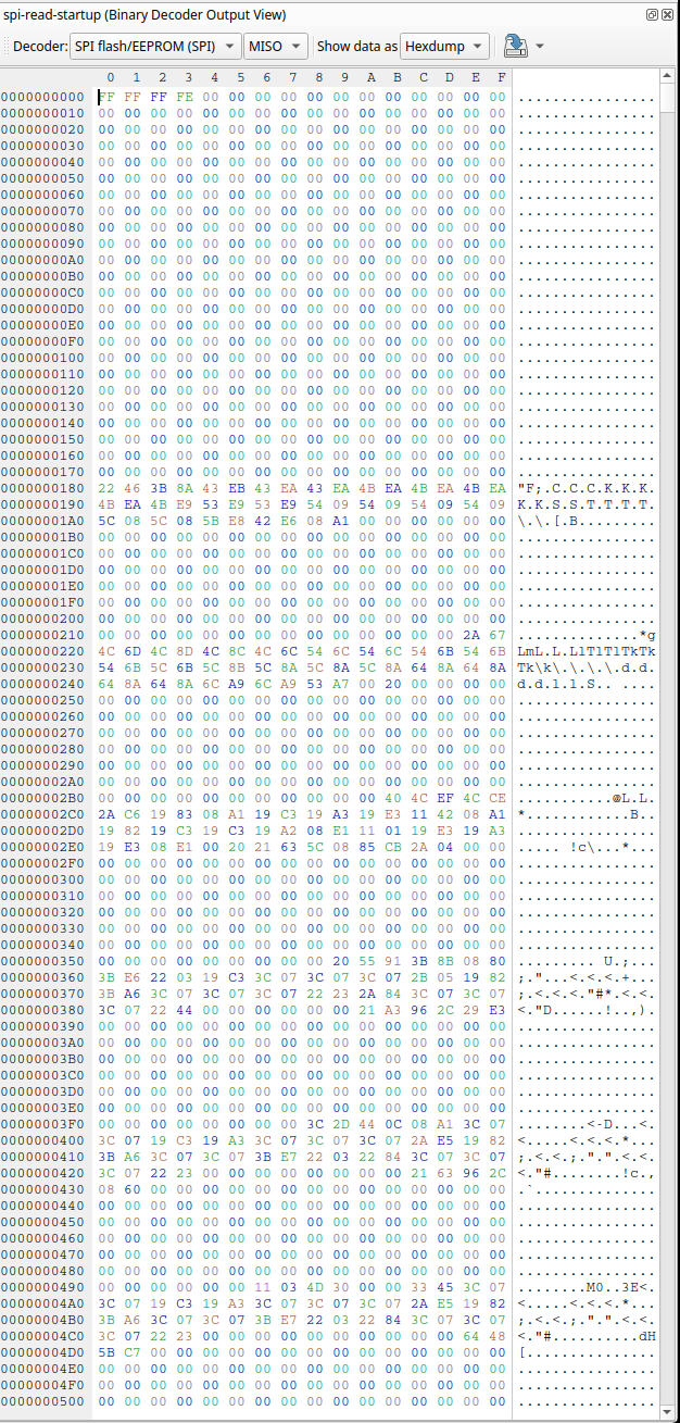
While this gives us some data, the CPU does not read all of the data in one shot; it reads data from this flash as needed. We can see this when we cycle through the menu options, which generates new traffic.
We need to dig a little deeper to get the full flash image without removing the chip.
Disabling the CPU
There are several ways for us to disable the CPU on this device:
- Locate a reset pin and pull it low
- Manipulate the external oscillator (if present) to keep the CPU from booting
- Manipulate an external interrupt or boot-mode pin on our target device to force it to boot into a different mode that will not access the SPI flash.
Luckily for us, this device has multiple labeled test pads, as seen in the image below:
Note: Reset pins are typically active low, but it is worth checking beforehand with a multi-meter to make sure that we don't damage anything before pulling something to the ground.
We can use this pin to hold the processor in reset if we hold the processor in reset and attempt to read out the flash in the same manner as before, we see the following:
pi@pifex:~/targets/toothbrush $ ./run-flashrom.sh r spi2.bin
flashrom unknown on Linux 6.6.74+rpt-rpi-v8 (aarch64)
flashrom is free software; get the source code at https://flashrom.org

Using clock_gettime for delay loops (clk_id: 1, resolution: 1ns).
Using default 2000kHz clock. Use 'spispeed' parameter to override.
===
SFDP has autodetected a flash chip which is not natively supported by flashrom yet.
All standard operations (read, verify, erase and write) should work, but to support all possible features we need to add them manually.
You can help us by mailing us the output of the following command to flashrom@flashrom.org:
'flashrom -VV [plus the -p/--programmer parameter]'
Thanks for your help!
===
Found Unknown flash chip "SFDP-capable chip" (8192 kB, SPI) on linux_spi.
===
This flash part has status UNTESTED for operations: WP
The test status of this chip may have been updated in the latest development
version of flashrom. If you are running the latest development version,
please email a report to flashrom@flashrom.org if any of the above operations
work correctly for you with this flash chip. Please include the flashrom log
file for all operations you tested (see the man page for details), and mention
which mainboard or programmer you tested in the subject line.
Thanks for your help!
Reading flash... done.
Now we have a binary image, and we can learn a little more about the internals of this toothbrush.
Note: When reading a SPI flash chip in-circuit, read it multiple times and check the MD5 of the results. This can confirm that you are getting consistent reads.
pi@pifex:~/targets/toothbrush $ md5sum spi.bin
1dca157fef51ea511c713c933963fa19  spi.bin
pi@pifex:~/targets/toothbrush $ md5sum spi2.bin
1dca157fef51ea511c713c933963fa19  spi2.bin
Firmware Analysis
The first step with any unknown binary blob is to run binwalk or unblob against it; binwalk produces the following:
pi@pifex:~/targets/toothbrush $ binwalk spi.bin

DECIMAL       HEXADECIMAL     DESCRIPTION
--------------------------------------------------------------------------------
If we run strings, we can see some data, but none of it shows up in our debug output. While this could be firmware, if we look at the raw data, we see the following:
pi@pifex:~/targets/toothbrush $ hexdump -C -n512 spi.bin
00000000  00 00 00 00 00 00 00 00  10 a2 6b 6d 94 b2 9c f3  |..........km....|
00000010  8c 71 52 aa 00 00 00 00  00 00 00 00 00 00 00 00  |.qR.............|
00000020  00 00 6b 6d ff ff ff ff  ff ff ff ff ff ff ff ff  |..km............|
00000030  f7 9e 31 a6 00 00 00 00  00 00 00 00 5a eb ff ff  |..1.........Z...|
00000040  ff ff ff ff ff ff ff ff  ff ff ff ff ff ff ff ff  |................|
00000050  21 04 00 00 00 00 00 00  e7 3c ff ff ff ff ce 59  |!........<.....Y|
00000060  31 86 18 c3 5a cb f7 be  ff ff ff ff a5 34 00 00  |1...Z........4..|
00000070  00 00 4a 69 ff ff ff ff  ff df 10 82 00 00 00 00  |..Ji............|
00000080  00 00 52 aa ff ff ff ff  ff df 10 82 21 24 8c 71  |..R.........!$.q|
00000090  ff ff ff ff ad 55 00 00  00 00 00 00 00 00 00 20  |.....U......... |
000000a0  ef 7d ff ff ff ff 42 28  4a 69 bd d7 ff ff ff ff  |.}....B(Ji......|
000000b0  84 10 00 00 00 00 00 00  00 00 00 00 c6 18 ff ff  |................|
000000c0  ff ff 6b 6d 63 2c d6 9a  ff ff ff ff 63 0c 00 00  |..kmc,......c...|
000000d0  00 00 00 00 00 00 00 00  ad 75 ff ff ff ff 8c 51  |.........u.....Q|
000000e0  73 ae de fb ff ff ff ff  5a cb 00 00 00 00 00 00  |s.......Z.......|
000000f0  00 00 00 00 9c f3 ff ff  ff ff 94 b2 7b cf e7 1c  |............{...|
00000100  ff ff ff ff 52 aa 00 00  00 00 00 00 00 00 00 00  |....R...........|
00000110  9c d3 ff ff ff ff 9c d3  73 ae de fb ff ff ff ff  |........s.......|
00000120  5a cb 00 00 00 00 00 00  00 00 00 00 9c f3 ff ff  |Z...............|
00000130  ff ff 94 b2 63 2c d6 9a  ff ff ff ff 63 2c 00 00  |....c,......c,..|
00000140  00 00 00 00 00 00 00 00  ad 75 ff ff ff ff 8c 51  |.........u.....Q|
00000150  4a 69 bd d7 ff ff ff ff  84 10 00 00 00 00 00 00  |Ji..............|
00000160  00 00 00 00 c6 18 ff ff  ff ff 6b 6d 21 04 8c 71  |..........km!..q|
00000170  ff ff ff ff ad 75 00 00  00 00 00 00 00 00 00 20  |.....u......... |
00000180  f7 9e ff ff ff ff 42 08  00 00 4a 49 ff ff ff ff  |......B...JI....|
00000190  ff df 10 a2 00 00 00 00  00 00 5a cb ff ff ff ff  |..........Z.....|
000001a0  ff df 08 61 00 00 00 00  e7 1c ff ff ff ff d6 9a  |...a............|
000001b0  39 e7 21 04 63 0c f7 be  ff ff ff ff a5 14 00 00  |9.!.c...........|
000001c0  00 00 00 00 5a cb ff ff  ff ff ff ff ff ff ff ff  |....Z...........|
000001d0  ff ff ff ff ff ff ff df  18 e3 00 00 00 00 00 00  |................|
000001e0  00 00 63 2c ff ff ff ff  ff ff ff ff ff ff ff ff  |..c,............|
000001f0  ef 7d 29 65 00 00 00 00  00 00 00 00 00 00 00 00  |.})e............|
If this were an ARM Cortex firmware image, we would expect to see an Interrupt Vector Table (IVT). On the Cortex-M, the vector table is preceded by a stack pointer, which will point to somewhere in the CPU's RAM. If we examine the memory map for our processor, we have the following:
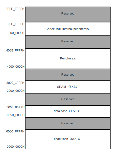
If this were a firmware image for this processor, we would expect to see a pointer to somewhere in the SRAM region and a table pointing to offsets in the internal flash; we do not. We also do not see any data that resembles ARM instructions, so what could this data be?
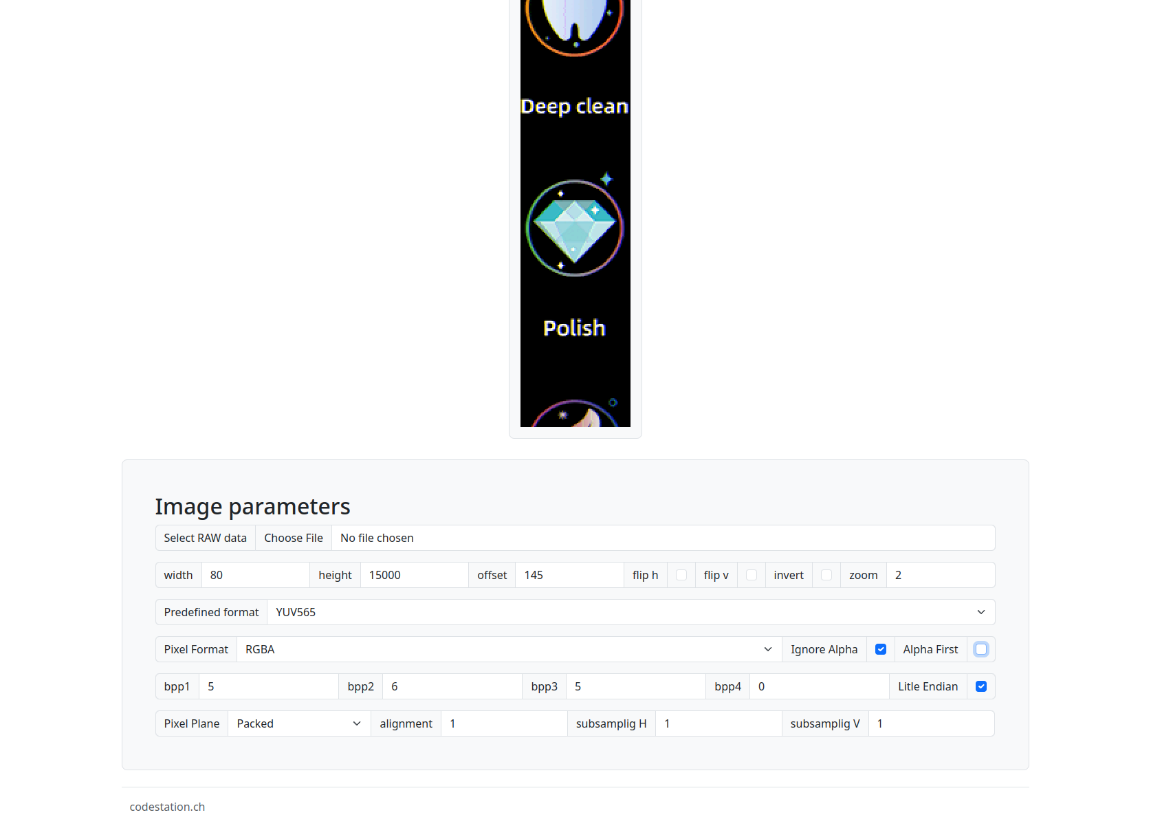
Recall that this device has a high-(ish) resolution screen, so this data is likely the image data displayed on startup. For devices with OLED displays, it is rare that the data is stored in a standard image format. It is often stored as pixelated RGB data, which can be difficult to parse. Luckily, there are tools available, such as https://codestation.ch/, that can allow us to test various formats and parameters.
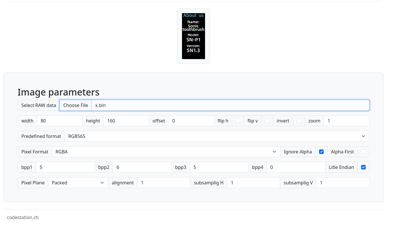
This introduces a new problem; we know very little about the formatting being used, so let's start with what we do know. The width and length of this screen are 11mm by 22mm, which means that our pixel ratio should be similar. Common ratios for these screens include 128x64; however, if we try that, it does not work. After some experimenting, a width of 80 and a height of 160 worked, and I could properly render the images on the screen. See the output below for more details:
Now that we know the size of the images and the screen layout, we can carve out the various images from the binary and load them as shown below. Using the data that we gathered earlier in pulseview, we know the offsets in the flash where som eof these images are stored.Each image was 24kb pixel maps (remember the read size from before?). Now that they are extracted, we should be able to replace them! After looking through the SPI flash image, it was determined that the bitmap for the software information screen is located at offset 0x308061 in our SPI flash image. It was individually extracted and loaded as shown below:
With all of this information, we can generate an RGB file from an 80x160-pixel image file and overwrite the SPI flash with our modified pixel map to display a custom image.
As a test, let's take a picture of everyone's favorite owl (Bubo from Clash of the Titans), scale it to 80x160, and then convert it to RGB565 with ffmpeg.
ffmpeg -i bubo.jpg -pix_fmt rgb565le test.rgb
This image was injected into the original SPI flash and re-flashed, as shown below:
flashrom -p linux_spi:dev=/dev/spidev0.0 -w flashme.bin
Result:
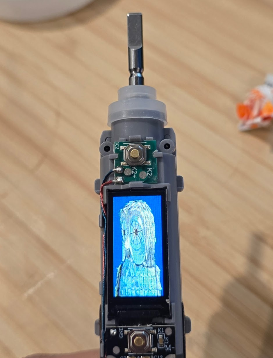
Our new image worked, and was displayed properly! We now understand how the SPI flash is structured, but we still have not extracted the firmware. We have one more source: the internal flash on the MCU. In our next post, we'll discuss how to communicate with an SWD interface and write an OpenOCD config file for a new microcontroller.
Conclusion
This series aims to show readers that there are many ways to get familiar with embedded systems reverse engineering without breaking the bank and that interesting targets can be found almost anywhere!
With this post, we've talked about:
- Configuring a Raspberry Pi image using the pifex-sw repository and pi-gen
- How to identify/instrument a UART even when no signals are active on the PCB
- Multiple methods for in-circuit SPI flash extraction
- Analyzing SPI traffic with Pulseview
- Extracting SPI flash via
flashrom
- Methods and tools for analyzing image files in an undocumented format
- Reflashing SPI flash chips with flashrom
Stay tuned for part three for a deep dive into using SWD to reprogram the flash on a microcontroller that is not directly supported by OpenOCD!
If you're interested in hardware security training at your organization, please don't hesitate to contact us. We also have a self-paced training available here
If you want to stay informed about official releases, new courses, and blog posts, sign up for our mailing list here.